
Consumable components inside semiconductor plasma-processing chambers are designed to operate in environments containing reactive radicals, energetic ions, elevated temperatures, repeated RF cycles and aggressive chamber-cleaning chemistry.
They are not expected to last indefinitely.
Focus rings, edge rings, electrodes, showerheads, liners, windows, nozzles, insulators and other plasma-facing parts gradually lose material, change surface condition or accumulate reaction products during operation.
The critical question for a fab or equipment engineer is therefore not simply:
How long should this part last?
A more useful question is:
At what point does component wear begin to increase particle risk, contamination, process drift or wafer yield loss?
For semiconductor consumables, the correct replacement point is usually determined by a combination of erosion, dimensional change, particle performance, surface condition and process stability rather than by a fixed number of operating hours.
This guide explains how plasma chamber consumables degrade, how their service life can be monitored and how buyers can define practical replacement and RFQ criteria.
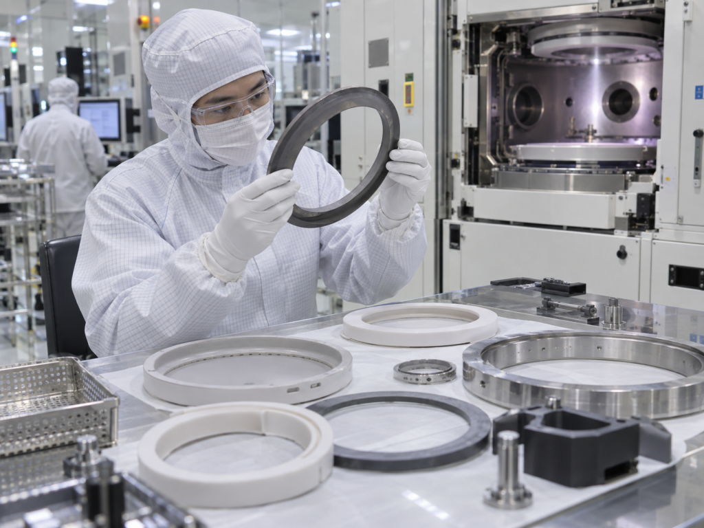
Why Semiconductor Chamber Consumables Wear Out
Plasma-facing components experience several degradation mechanisms simultaneously.
The most important are:
- Chemical erosion
- Physical sputtering
- Ion bombardment
- Surface fluorination or chlorination
- Cicli termici
- Polymer deposition
- Cleaning-cycle attack
- Particle redeposition
- Mechanical handling damage
Reactive plasma attacks not only the wafer but also surfaces surrounding the plasma.
In fluorine-based environments, for example, internal ceramic materials can undergo chemical reactions and physical erosion. Research on Al₂O₃, Y₂O₃, YF₃ and YOF surfaces shows that plasma-material reactions can change surface chemistry, roughness and particle-generation behavior.
The resulting component degradation can eventually affect both tool performance and wafer quality.
Which Semiconductor Components Are Normally Considered Consumables?
The exact list depends on equipment design, but common plasma-processing consumables include:
Focus Rings and Edge Rings
These components surround the wafer and help control the electric field and plasma distribution near the wafer edge.
Their geometry is therefore directly related to edge-process uniformity.
Materials may include:
- Silicio
- CVD silicon carbide
- Quarzo
- Advanced ceramics
Focus rings are particularly sensitive because erosion changes their height and profile relative to the wafer and electrostatic chuck.
Commercial semiconductor ceramic suppliers describe focus and edge rings as components used specifically to control etch uniformity around the wafer perimeter.
Upper Electrodes
Silicon or other plasma-compatible materials may be used in electrodes exposed directly to reactive plasma.
Erosion can alter:
- Electrode thickness
- Gas-hole geometry
- Surface profile
- Plasma characteristics
Showerheads and Gas Distribution Components
These components must maintain precise gas distribution while resisting plasma and corrosive process gases.
Critical changes can include:
- Hole enlargement
- Hole blockage
- Surface erosion
- Deposits
- Dimensional distortion
Chamber Liners
Liners protect the underlying chamber structure.
Depending on the process, they may use:
- Allumina
- Yttria-coated aluminum
- Other yttrium-based coatings
- Quarzo
- Carburo di silicio
RF and Microwave Windows
A plasma chamber window must combine plasma resistance with appropriate electrical characteristics.
Excessive erosion, deposition or surface damage can influence energy transmission and temperature distribution.
Ceramic Insulators and Structural Components
Alumina and other engineered ceramics are widely used where electrical insulation, mechanical strength and vacuum compatibility are required.
These parts may not always be directly exposed to the most intense plasma, but contamination, coating degradation or edge damage can still determine their usable lifetime.
What Does “Consumable Lifetime” Actually Mean?
Consumable lifetime should not automatically mean calendar time.
A component may be installed for six months in a low-utilization R&D tool but accumulate less plasma exposure than another component experiences in several weeks of high-volume manufacturing.
More useful lifetime metrics include:
RF hours
Total hours of actual plasma exposure.
Wafer count
Number of wafers processed while the component is installed.
Process cycles
Number of deposition, etch or cleaning sequences.
Cleaning cycles
Number of aggressive in-situ or wet-clean cycles.
Material loss
Measured dimensional reduction at critical locations.
Process performance
Changes in etch rate, uniformity or another chamber parameter.
Particle performance
Increase in particle adders attributed to chamber condition.
A serious lifetime program normally tracks several of these at the same time.
Why Fixed Lifetime Numbers Can Be Misleading
It is tempting to request:
“Focus ring lifetime: 500 hours.”
But two nominally identical focus rings may experience very different wear rates.
Lifetime depends on variables such as:
- Plasma chemistry
- RF power
- Bias power
- Pressure
- Temperatura
- Gas composition
- Chamber location
- Wafer recipe
- Cleaning chemistry
- Duty cycle
- Component geometry
- Material purity
- Grain structure
- Coating properties
- Finitura superficiale
Historical plasma-chamber literature has documented consumable lifetimes around hundreds of RF hours for certain quartz and silicon parts, but such values belong to specific chamber and process conditions and should not be treated as universal industry specifications.
For procurement, the customer’s existing chamber conditions are much more useful than a generic lifetime claim.
1. Plasma Erosion: The Most Visible Lifetime Mechanism
Plasma erosion gradually removes material from the surface of the component.
The mechanism can include both:
Chemical reaction
Reactive radicals interact with the material and form reaction products.
e
Physical sputtering
Energetic ions physically remove atoms or reaction products from the surface.
The balance between these mechanisms depends on the plasma chemistry and local ion energy.
Recent studies comparing chamber-protection ceramics demonstrate that fluorocarbon plasma can produce substantially different erosion behavior depending on surface chemistry and material composition.
Why Erosion Is More Than a Cosmetic Problem
A component does not need to fracture before it becomes unusable.
Small dimensional changes can affect the process.
For example, focus-ring erosion may change:
- Ring height
- Wafer-to-ring step
- Edge electric field
- Plasma sheath shape
- Edge etch rate
- Critical dimension uniformity
Likewise, erosion of gas distribution holes can alter local gas flow.
Therefore, replacement criteria should be linked to functional dimensions, not merely visible damage.
2. Particle Generation Is Often a More Important Warning Than Material Loss
A component may still retain most of its original thickness but begin producing unacceptable particles.
Particles can originate from:
- Plasma-eroded surfaces
- Fluoride reaction layers
- Polymer deposits
- Coating delamination
- Microfratture
- Pitting
- Redeployed chamber material
- Mechanical damage
- Cleaning residues
Research into fluorine-plasma exposure has shown that reactions occurring on chamber coatings can generate contamination particles, while accumulated particles or deposits may later detach from the surface and reach the wafer.
This means a component should not automatically remain in service simply because its dimensions still pass inspection.
Particle performance can become the controlling replacement criterion.
3. Why Surface Roughening Matters
Plasma attack rarely removes material perfectly uniformly.
As exposure accumulates, surfaces may become:
- Rough
- Pitted
- Textured
- Porous
- Locally cracked
Surface roughness changes can influence both erosion and deposition behavior.
A rough surface provides more area and more locations where reaction products or process polymers may accumulate.
Eventually, these deposits can become unstable.
Older high-density plasma studies of quartz components, for example, linked quartz surface pitting and temperature-related polymer flaking with particle generation.
Therefore, monitoring only total material loss can overlook an important failure mechanism.
4. Polymer Buildup Can Limit Lifetime Even When the Base Material Is Intact
Not every consumable fails because it is etched away.
During many plasma processes, films or polymeric byproducts accumulate on chamber surfaces.
Initially, deposition may be stable.
After repeated processing and cleaning cycles, however, the film may:
- Become thicker
- Crack
- Powder
- Delaminate
- Flake
A component can therefore become a particle source even if the underlying substrate remains dimensionally acceptable.
The relevant lifetime question becomes:
How many process and clean cycles can the surface tolerate before deposited films become unstable?
This is why cleaning history should be included in consumable tracking.
5. Contamination Can End Component Life Before Mechanical Failure
In advanced semiconductor manufacturing, contamination tolerance may be extremely low.
Potential contamination can include elements originating from:
- Base material
- Rivestimento
- Machining
- Pulizia
- Handling
- Imballaggio
- Plasma reaction products
Consumable erosion has long been recognized as a possible source of particulate and elemental contamination inside plasma-processing equipment.
This becomes especially important when a chamber component contains elements that are sensitive to the particular device process.
Therefore, a component can fail qualification even though:
- It is not cracked
- Its dimensions remain acceptable
- It still functions mechanically
If elemental contamination exceeds the process limit, its useful service life is over.
6. Plasma Chemistry Strongly Changes Consumable Lifetime
There is no single material that offers maximum lifetime under every plasma environment.
Different process gases interact differently with chamber materials.
Common plasma chemistries include:
- Fluorocarbon
- Fluorine
- Chlorine
- Bromine
- Oxygen
- Argon-containing mixtures
Fluorine-based processes are especially relevant to ceramic chamber protection.
Research shows that Al₂O₃, Y₂O₃, YF₃ and YOF can exhibit significantly different chemical and physical erosion behaviors under fluorocarbon plasma.
A 2025 study examining NF₃-based plasma also found that erosion and redeposition behavior differed according not only to coating material but also to the component’s location within the chamber.
This is an important procurement point:
Material selection should consider where the component is installed, not merely which gases exist somewhere in the chamber.
Silicon Consumables: What Determines Their Lifetime?
High-purity silicon is widely used in plasma-facing components where material compatibility with silicon wafer processing is important.
Typical components include:
- Anelli di messa a fuoco
- Anelli per bordi
- Electrodes
- Rings surrounding the wafer
Silicon can offer contamination advantages in selected silicon-processing environments.
However, its surface is still consumed by plasma.
Important lifetime indicators include:
- Thickness loss
- Ring-height change
- Groove erosion
- Hole-size change
- Profilo del bordo
- Surface pitting
For precision rings, even relatively small dimensional changes can become process-relevant before a large fraction of the material has disappeared.
CVD SiC Consumables: Longer Life Is Not the Only Requirement
CVD silicon carbide is attractive for many demanding semiconductor chamber components because it combines:
- High purity
- Elevata durezza
- Good thermal properties
- Strong plasma resistance in many environments
It is commonly considered for high-value focus rings and other components where longer dimensional stability can justify higher material cost.
However, CVD SiC quality must be considered together with:
- Densità
- La purezza
- Microstructure
- Finitura superficiale
- Machining quality
- Qualità dei bordi
A theoretically plasma-resistant material will not perform optimally if the finished component contains subsurface damage, chipped edges or contaminated machining surfaces.
Therefore, comparing consumables purely by raw material name can be misleading.
Quartz Consumables: Monitor Pitting and Surface Condition
High-purity quartz remains important in semiconductor equipment because of its:
- High chemical purity
- Isolamento elettrico
- Optical characteristics
- Established fabrication processes
But quartz can experience significant attack in some fluorine-rich plasma environments.
Potential lifetime indicators include:
- Surface recession
- Pitting
- Frosting
- Loss of transparency
- Microcracking
- Polymer accumulation
- Generazione di particelle
Older plasma-processing research specifically reported that high-density plasma erosion and thermal behavior could contribute to quartz pitting and particle problems under certain oxide-etch conditions.
Therefore, quartz lifetime should be evaluated for the actual chamber chemistry rather than generalized across all tools.
Alumina and Plasma-Resistant Ceramic Components
High-purity alumina offers:
- Isolamento elettrico
- Mechanical strength
- Dimensional stability
- Established semiconductor-equipment use
However, direct exposure to aggressive fluorine plasma can change the surface chemistry of alumina.
For more demanding plasma regions, chamber components may therefore use protective materials such as:
- Y₂O₃
- YF₃
- YOF
- Other yttrium-containing systems
Research published in 2024–2026 continues to focus heavily on improving erosion resistance and reducing contamination particles from these ceramic surfaces.
This illustrates an important trend:
For advanced chamber consumables, particle behavior can be as important as the nominal erosion rate.
Coating Lifetime Should Be Treated Separately from Component Lifetime
For coated chamber parts, several different failures are possible.
The coating may:
- Erode uniformly
- Become chemically modified
- Crack
- Delaminate
- Develop pores
- Lose adhesion
- Generate particles
Meanwhile, the underlying structural component may remain completely usable.
For this reason, it is useful to separate:
Substrate lifetime
from
coating service interval
e
refurbishment limit.
A coated component may be cleaned and recoated several times if the base geometry remains within specification.
But refurbishment should not be unlimited.
Repeated coating removal, blasting, machining or chemical treatment can eventually change dimensions or damage the substrate.
Cleaning Cycles Can Consume the Consumable Too
Maintenance is intended to restore chamber condition, but cleaning itself contributes to component aging.
Depending on the component, cleaning may involve:
- In-situ plasma cleaning
- Wet chemical cleaning
- Pulizia ad ultrasuoni
- Mechanical treatment
- Surface stripping
- Recoating
Aggressive cleaning can:
- Remove material
- Change roughness
- Attack coatings
- Enlarge microscopic defects
- Introduce chemical residue
- Cause edge damage
Research on plasma-resistant Y₂O₃ surfaces has specifically investigated how cleaning procedures interact with particle contamination, demonstrating that post-process cleaning should be treated as part of the component’s performance history rather than a neutral event.
Therefore, suppliers and fabs should track both plasma exposure and cleaning count.
Seven Practical Signs That a Consumable May Need Replacement
There is rarely one universal indicator.
A stronger replacement strategy combines several warning signals.
1. Critical Dimension Reaches the Lower Limit
Tra gli esempi figurano:
- Focus-ring height
- Electrode thickness
- Diametro del foro
- Wall thickness
- Groove depth
Dimensional limits should ideally come from tool or process qualification rather than visual judgment.
2. Particle Adders Increase
A sustained particle increase after chamber conditioning can indicate deteriorating internal surfaces.
Particle excursions should be correlated with:
- Component age
- Chamber position
- Recent cleaning
- Recipe changes
- Maintenance history
3. Process Uniformity Begins to Drift
Changing component geometry can alter the plasma.
Possible symptoms include:
- Edge etch-rate change
- Across-wafer nonuniformity
- CD drift
- Selectivity change
- Center-to-edge variation
For focus rings especially, process drift can become a lifetime criterion.
4. Surface Roughness or Pitting Increases
Significant roughening can increase deposit instability and particle risk.
5. Coating Damage Becomes Visible
Cracks, exposed substrate or localized coating loss may require immediate evaluation.
6. Contamination Exceeds the Allowable Limit
Elemental contamination can determine replacement even when the part is mechanically sound.
7. The Component Reaches the Qualified Preventive-Maintenance Limit
Once sufficient production data exist, fabs may establish a preventive replacement interval before measurable yield degradation occurs.
RF Hours vs Wafer Count: Which Lifetime Metric Is Better?
Neither is perfect by itself.
RF Hours
RF hours represent actual plasma exposure more accurately than calendar time.
But one RF hour under a mild recipe is not equivalent to one RF hour under aggressive high-bias plasma.
Wafer Count
Wafer count is easy to track and relates directly to production throughput.
But different recipes can create radically different component wear per wafer.
Cleaning Cycles
Cleaning count is particularly important for surfaces exposed to aggressive chamber-clean gases.
Dimensional Loss
Physical measurements directly show component wear.
However, measurement requires maintenance access and may not detect contamination or particle instability.
The strongest method is therefore to build a multi-variable lifetime history:
RF hours + wafer count + recipe mix + cleaning cycles + dimensional inspection + particle trend + process trend
This gives a much more meaningful consumable-lifetime model than a single number.
How to Build a Consumable Lifetime Curve
For a new focus ring, electrode or ceramic liner, establish the initial condition before installation.
Record:
- Initial dimensions
- Weight if useful
- Rugosità superficiale
- Photographs
- Surface appearance
- Material lot
- Manufacturing lot
During scheduled maintenance, repeat measurements.
Ad esempio:
New component
→ Baseline inspection
After initial production period
→ Measure erosion
Mid-life
→ Check dimensions + particles + process data
Near expected end of life
→ Increase inspection frequency
Removed component
→ Final dimensional and surface analysis
This creates an erosion curve for the actual chamber.
After several component lots, the fab can establish a much more reliable preventive-maintenance window.
Replacement Should Be Based on the Earliest Critical Failure Mode
Suppose a focus ring has:
70% dimensional life remaining,
but particle performance already exceeds the fab specification.
Its usable lifetime is finished.
Another component may have:
excellent particle performance,
but the ring height has changed enough to affect edge etch uniformity.
Its usable lifetime is also finished.
Therefore:
Consumable lifetime = the point at which the first critical process, contamination, particle or dimensional limit is reached.
This approach is more meaningful than asking how much material remains.
What Should Be Included in an Incoming Inspection?
For high-value semiconductor consumables, incoming inspection can include:
Material Verification
- Material type
- La purezza
- Densità
- Electrical properties if required
Dimensional Inspection
- OD
- ID
- Spessore
- Piattezza
- Parallelismo
- Groove geometry
- Hole dimensions
- Position tolerances
Surface Inspection
- Roughness
- Graffi
- Pits
- Chipping
- Tool marks
- Contaminazione superficiale
Ceramic Inspection
When applicable:
- Porosità
- Grain structure
- Densità
- Coating thickness
- Coating adhesion
- Coating uniformity
Cleanliness
Depending on process sensitivity:
- Particle cleanliness
- Metal contamination
- Ionic residue
- Condizioni della confezione
A component that begins service with a poorly controlled surface can have a substantially different lifetime from an otherwise identical part manufactured to a stable finish.
Recommended RFQ Specifications for Plasma Chamber Consumables
A useful RFQ should include more than the component name.
1. Component Identification
Component name:
Focus ring / edge ring / electrode / showerhead / liner / window / insulator / other
Equipment platform:
Tool manufacturer and chamber model if disclosure is permitted
Part number:
OEM or customer reference number
Drawing:
2D drawing and 3D model where available
2. Material
Required material:
Silicon / CVD SiC / fused quartz / alumina / coated ceramic / other
Material grade:
Specify if known
Purity:
Define required minimum purity
Prohibited elements:
Specify contamination-sensitive elements
3. Plasma Environment
Process:
Etch / deposition / cleaning / other
Primary chemistry:
CF₄ / CHF₃ / C₄F₆ / SF₆ / NF₃ / Cl₂ / HBr / O₂ / Ar / other
RF power:
Typical operating range
Bias power:
If relevant
Operating temperature:
Typical range
Pressure:
Typical process range
Plasma exposure:
Direct / partial / shielded
4. Critical Dimensions
Identify which dimensions determine usable lifetime.
Examples:
- Ring height
- Wall thickness
- Hole size
- Groove depth
- Piattezza
- Parallelismo
Do not apply identical tolerances to every feature if only certain dimensions are process-critical.
5. Surface Requirements
Specify:
- Rugosità superficiale
- Polishing condition
- Lapped or ground areas
- Edge-break requirements
- Maximum allowable chips
- Cleaning condition
6. Coating Requirements
For coated components:
- Coating material
- Coating thickness
- Uniformità dello spessore
- Porosity requirement
- Rugosità superficiale
- Adhesion requirement
- Maximum exposed substrate
- Recoating eligibility
7. Cleanliness Requirements
Define:
- Final cleaning procedure
- Particle limit
- Metal contamination requirement
- Packaging method
- Cleanroom requirement
8. Inspection Documentation
Request as required:
- Material certificate
- Dimensional report
- Surface roughness report
- Purity data
- Coating thickness report
- Particle inspection
- Photographs
- Certificate of Conformance
9. Lifetime Information
Instead of simply asking:
“Lifetime ≥ 1,000 hours,”
provide the actual operating conditions and ask for:
- Existing reference life under similar chemistry
- Expected primary wear mechanism
- Recommended inspection interval
- Critical replacement dimension
- Refurbishment possibility
This gives the supplier a much better basis for technical evaluation.
What Information Should You Send When Replacing an Existing OEM Part?
Reverse-engineering or qualifying an alternative semiconductor consumable becomes much easier when the supplier receives both the new and used-part information.
Useful information includes:
- OEM part number
- Disegno
- Original material
- Tool model
- Plasma chemistry
- RF power
- Current service life
- Current failure mode
- New-part dimensions
- Used-part dimensions
- Photographs of worn areas
- Particle problem description
- Process drift data
- Required improvement target
Ad esempio:
“Current silicon focus ring lasts approximately X RF hours before edge-uniformity drift.”
is far more useful than:
“Please manufacture a silicon ring.”
The worn component shows where the chamber actually consumes material.
Can a Higher-Cost Material Reduce Total Cost?
Yes, but only if the full cost of ownership is considered.
Consumable cost includes more than purchase price.
The real cost can include:
Part price
Chamber downtime
Maintenance labor
Chamber conditioning wafers
Lost production
Particle excursions
Perdita di resa
A more expensive CVD SiC or advanced ceramic component may make economic sense if it significantly increases maintenance intervals or stabilizes the process.
On the other hand, a lower-cost material may remain preferable in a less aggressive chamber where component wear is not the limiting factor.
Therefore, material selection should be based on:
Cost per stable process hour
rather than simply:
Cost per component.
Why the Longest Lifetime Is Not Always the Best Consumable
Maximum erosion resistance does not automatically mean maximum process performance.
Changing component material can alter:
- Plasma chemistry
- Wall recombination
- Electrical properties
- RF coupling
- Thermal behavior
- Contamination species
- Process seasoning
Recent research on NF₃ plasma exposure illustrates that different yttrium-based surfaces can show different erosion and redeposition behavior depending on chamber position.
A material that lasts longer mechanically may therefore require process requalification.
For production equipment, the best consumable is the one that provides the optimum combination of:
- Stable plasma behavior
- Low particles
- Bassa contaminazione
- Predictable erosion
- Sufficient lifetime
- Reliable manufacturing consistency
- Acceptable cost
A Practical Consumable Replacement Strategy
A useful lifetime-management system can follow this sequence:
1. Define the critical component dimension
↓
2. Record the new-part baseline
↓
3. Track RF hours and wafer count
↓
4. Track process and cleaning recipes
↓
5. Monitor particles and process uniformity
↓
6. Inspect the component during PM
↓
7. Calculate erosion rate
↓
8. Correlate wear with wafer performance
↓
9. Establish warning and replacement limits
↓
10. Refine the PM interval using multiple component lots
This converts consumable replacement from an experience-based decision into a data-driven process.
Conclusione
Semiconductor wafer-processing consumables should not be replaced according to calendar age alone.
Plasma-facing components gradually change through:
- Chemical erosion
- Physical sputtering
- Surface roughening
- Plasma-material reactions
- Polymer buildup
- Generazione di particelle
- Coating degradation
- Cleaning-cycle damage
The usable lifetime ends when the first critical limit is reached.
That limit may be:
maximum dimensional loss,
maximum particle level,
maximum contamination level,
maximum process drift,
oppure
a qualified preventive-maintenance interval.
For focus rings, electrodes, showerheads, liners, quartz components and plasma-resistant ceramic parts, the most reliable lifetime strategy combines component inspection with RF hours, wafer count, cleaning cycles and actual wafer-process data.
When sourcing replacement consumables, RFQs should therefore specify not only material and dimensions but also the real plasma environment, critical wear dimensions, cleanliness requirements, surface condition and inspection documentation.
The objective is not simply to manufacture a component that fits the chamber.
It is to manufacture a consumable that maintains stable plasma conditions, minimizes particle and contamination risk, and delivers predictable performance throughout its qualified service life.