

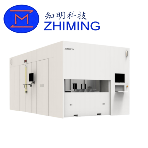
 The Ai250 (Medium Beam) ion implantation system is designed for 6-inch and 8-inch silicon wafer semiconductor manufacturing lines. It is a medium current ion implanter used in advanced integrated circuit fabrication processes, providing stable beam performance, high implantation accuracy, and reliable dose control.
The system supports an energy range from 5 keV to 250 keV, enabling both shallow and deep ion implantation applications. It is suitable for a wide range of semiconductor doping processes and is fully compatible with LSI manufacturing requirements.
Features
Stable Medium Beam Performance
Ensures stable ion beam output during long production cycles, improving process consistency and reducing variability.
Wide Energy Range Capability
Energy range of 5–250 keV supports flexible implantation requirements for different device structures and process nodes.
High Precision Process Control
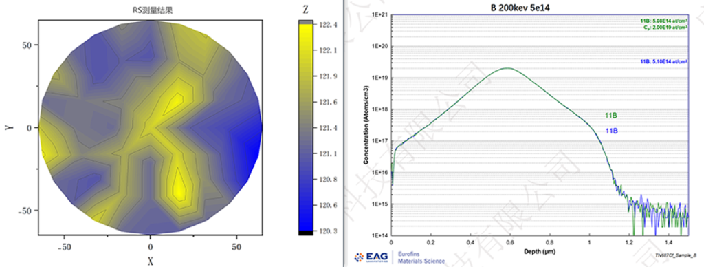
Provides high accuracy implantation performance with angle accuracy ≤ 0.2°, beam parallelism ≤ 0.2°, uniformity ≤ 0.5%, and repeatability ≤ 0.5%.
High Throughput Capability
Supports ≥ 200 wafers per hour, suitable for medium to high volume semiconductor production.
Pattern Implant Function
Supports multi-zone and quadrant implantation on a single wafer, improving process flexibility and reducing development cost.
LSI Process Compatibility
Fully compatible with LSI semiconductor manufacturing processes.
Specifiche principali
Process Parameters
| Articolo | Specifiche |
|---|---|
| Dimensione del wafer | 6–8 inch silicon wafers |
| Energy Range | 5–250 keV |
| Implanted Elements | B+, P+, As+, Ar+, N+, H+ |
| Dose Range | 5E11–1E16 ions/cm² |
Beam Performance
| Articolo | Specifiche |
|---|---|
| Maximum Beam Current | Ar+ ≥ 1300 μA @ ≥220 keV B+ ≥ 1000 μA @ ≥220 keV P+ ≥ 1300 μA @ ≥220 keV N+ ≥ 1000 μA @ ≥220 keV |
| Beam Stability | ≤ 15% / hour (beam interruption and arcing ≤ 1 time per hour) |
| Beam Parallelism | ≤ 0.2° |
Implantation Accuracy
| Articolo | Specifiche |
|---|---|
| Implant Angle Range | 0°–45° |
| Angle Accuracy | ≤ 0.2° |
| Uniformity (1σ) | ≤ 0.5% (B+, 2E14, 150 keV) |
| Repeatability (1σ) | ≤ 0.5% |
System Performance
| Articolo | Specifiche |
|---|---|
| Produttività | ≥ 200 wafers per hour |
| Livello di vuoto | < 5E-7 Torr |
| X-ray Leakage | ≤ 0.6 μSv/h |
| Scanning Mode | Horizontal electrostatic scanning + vertical mechanical scanning |
| Equipment Size | 5600 × 3300 × 2600 mm |
Application Fields
Semiconductor Device Manufacturing
Used in CMOS logic device production, providing precise dopant implantation for transistor formation.
Integrated Circuit Fabrication
Applied in LSI and advanced IC manufacturing processes requiring high precision doping control.
Shallow and Deep Junction Formation
Supports implantation processes for source/drain engineering and junction depth control.
Dopant Engineering
Used for controlling electrical properties of silicon wafers through accurate ion implantation.
Process Development and R&D
Suitable for semiconductor process development, pilot production, and experimental device fabrication.
Domande frequenti
1. What wafer sizes does the Ai250 support
The system supports 6-inch and 8-inch silicon wafers and is suitable for mainstream semiconductor manufacturing lines.
2. What is the energy range of the system
The energy range is 5 keV to 250 keV, supporting both shallow and deep implantation processes for semiconductor device fabrication.
3. What level of process accuracy does the system provide
The system provides angle accuracy within 0.2°, beam parallelism within 0.2°, and uniformity and repeatability within 0.5%, ensuring stable and high-yield production performance.
Recensioni
Ancora non ci sono recensioni.