
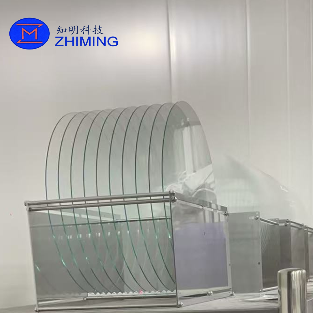
Glass wafers are becoming increasingly important in advanced semiconductor packaging, optical devices, MEMS, RF components, microfluidic chips, and through-glass via applications. Compared with silicon, glass offers excellent electrical insulation, high dimensional stability, optical transparency, low dielectric loss, and good compatibility with wafer-level packaging processes. As packaging structures become more complex, glass wafers often require precise holes, cavities, through-openings, or edge features. This makes glass wafer coring an essential processing step.
Glass wafer coring refers to the controlled removal of material from a glass wafer to create circular or customized holes. These holes may be used for alignment, fluid channels, optical paths, mechanical mounting, electrical isolation, or as preparation for further via formation. Although the concept appears simple, coring glass at wafer level is technically challenging because glass is hard, brittle, and sensitive to stress concentration. Poor coring quality can lead to edge chipping, microcracks, dimensional deviation, particle contamination, and even wafer breakage.
For semiconductor packaging, the quality of the cored hole directly affects device reliability, bonding yield, cleaning performance, and downstream process compatibility. Therefore, hole quality, edge chipping control, and tolerance management are key factors that engineers and buyers should evaluate when specifying glass wafer coring services.
1. Why Glass Wafer Coring Matters in Semiconductor Packaging
In advanced packaging, wafers are no longer simple flat carriers. They may function as interposers, optical substrates, MEMS platforms, redistribution carriers, or insulating support structures. Glass wafer coring is often required when a package design needs precise through-holes or cavities.
Typical applications include:
- Through-holes for alignment and assembly
- Openings for optical transmission or sensing
- Fluidic channels in MEMS and lab-on-chip devices
- Cavities for device clearance or encapsulation
- Mechanical positioning holes for wafer handling
- Preparation of glass substrates for advanced packaging structures
- Customized holes for wafer-level bonding or interposer design
Because many of these applications involve high-precision assembly, even small defects around the hole edge may affect yield. A minor crack may expand during thermal cycling. A rough hole wall may trap particles. Excessive edge chipping may reduce bonding area or interfere with sealing. For this reason, glass coring should be treated as a precision semiconductor process rather than a simple mechanical drilling operation.
2. Material Characteristics of Glass Wafers
Glass wafers used in semiconductor applications may include borosilicate glass, fused silica, quartz glass, aluminosilicate glass, alkali-free glass, and specialty glass materials. Each material has different mechanical, thermal, and optical properties.
Important material factors include:
| Material Factor | Influence on Coring |
|---|---|
| Durezza | Affects tool wear and cutting speed |
| Brittleness | Determines crack and chipping risk |
| Thermal expansion coefficient | Influences stress under heat |
| Wafer thickness | Affects hole wall quality and processing time |
| Surface roughness | Influences bonding and inspection requirements |
| Internal stress | May increase fracture risk during coring |
| Glass composition | Affects laser, abrasive, or mechanical processing behavior |
For example, fused silica has excellent thermal and optical properties but is hard and requires careful process control. Borosilicate glass is widely used in packaging and MEMS because of its good processability and stable properties. Alkali-free glass is often selected for electronic applications where ionic contamination must be minimized.
Before coring, engineers should confirm the glass type, wafer diameter, thickness, surface condition, and required cleanliness level. These parameters influence the processing method and achievable tolerance.
3. Main Methods for Glass Wafer Coring
Several technologies can be used to create holes in glass wafers. The choice depends on hole diameter, wafer thickness, edge quality, cost, throughput, and downstream requirements.
3.1 Mechanical Diamond Coring
Mechanical coring uses diamond tools to remove glass material by grinding. It is suitable for relatively large holes and can provide stable dimensional control when the process is well optimized. Diamond coring is commonly used when hole diameters are larger than typical laser-drilled microvias.
I vantaggi includono:
- Good dimensional control
- Suitable for thicker glass wafers
- Capable of producing clean circular holes
- Cost-effective for certain hole sizes and batch production
Le sfide includono:
- Edge chipping risk
- Tool wear
- Process-induced stress
- Need for optimized feed rate, spindle speed, and coolant control
3.2 Ultrasonic-Assisted Machining
Ultrasonic machining uses high-frequency vibration combined with abrasive action to reduce cutting force. It is useful for brittle materials such as glass, quartz, sapphire, and ceramics.
I vantaggi includono:
- Riduzione delle sollecitazioni meccaniche
- Lower risk of large cracks
- Better control for brittle materials
- Suitable for high-precision holes
Le sfide includono:
- Slower processing speed
- Equipment cost
- Need for careful abrasive and tool control
3.3 Laser Drilling or Laser-Assisted Processing
Laser processing can create small holes or microfeatures in glass. It is especially useful for microvia formation, but thermal effects must be controlled.
I vantaggi includono:
- High flexibility
- Suitable for small holes
- No direct tool contact
- Compatible with complex patterns
Le sfide includono:
- Heat-affected zones
- Microfratture
- Tapered hole profiles
- Possible recast or debris formation
- Need for post-cleaning or polishing
3.4 Abrasive Waterjet or Hybrid Methods
For some large openings or special shapes, abrasive waterjet or hybrid methods may be considered. However, for semiconductor-grade wafers, cleanliness, edge quality, and microcrack control must be carefully evaluated.
4. Hole Quality: What Should Be Evaluated?
Hole quality is not only about whether the hole is successfully formed. In semiconductor packaging, the hole must meet functional, dimensional, and reliability requirements.
Key quality indicators include:
4.1 Hole Diameter Accuracy
The actual hole diameter should match the design requirement within the specified tolerance. Diameter accuracy is influenced by tool size, tool wear, vibration, wafer thickness, and process parameters.
For precision glass wafer coring, both entrance and exit diameters should be measured because brittle materials may show slight taper or edge breakout.
4.2 Roundness
Roundness describes how close the hole is to a perfect circle. Poor roundness can affect alignment, assembly, or sealing. It may be caused by tool vibration, uneven material removal, or unstable wafer fixation.
4.3 Hole Position Accuracy
Position accuracy is critical when holes are used for alignment, bonding, or multi-wafer assembly. Even if the hole diameter is correct, positional deviation can lead to packaging misalignment.
4.4 Hole Wall Roughness
The inner wall of a cored glass hole may have grinding marks, microcracks, or rough surfaces. Excessive roughness can affect cleaning, bonding, coating, or fluid flow in microfluidic applications.
4.5 Entrance and Exit Edge Condition
The entrance and exit edges are the most vulnerable areas. Chipping, cracks, and breakout often occur near these edges because stress concentrates during tool entry and exit.
4.6 Microcrack Inspection
Microcracks may not be obvious under normal visual inspection, but they can expand during thermal cycling, chemical cleaning, bonding, or mechanical loading. Optical microscopy, polarized light inspection, or other inspection methods may be used depending on application requirements.
5. Edge Chipping: Causes and Control Methods
Edge chipping is one of the most common defects in glass wafer coring. It appears as small fragments broken away from the hole edge. In severe cases, chipping may reduce effective bonding area, create particles, or become a crack initiation point.
5.1 Main Causes of Edge Chipping
Common causes include:
- Excessive feed rate
- Improper spindle speed
- Tool wear or poor tool quality
- Insufficient coolant or lubrication
- Poor wafer support
- Excessive vibration
- High internal stress in the glass
- Incorrect entry or exit strategy
- Inappropriate processing method for wafer thickness
Because glass fails by brittle fracture, even small process instability may create chips or cracks.
5.2 Entry-Side and Exit-Side Chipping
Exit-side chipping is often more severe than entry-side chipping. As the tool breaks through the bottom surface, the remaining glass thickness becomes thin and less supported. This can cause sudden breakout.
To reduce exit chipping, manufacturers may use:
- Sacrificial backing plates
- Double-sided processing
- Lower feed rate near breakthrough
- Optimized tool geometry
- Controlled coolant delivery
- Step coring or staged material removal
5.3 Tool Condition and Diamond Grit Size
Tool quality strongly affects edge quality. A worn diamond tool may increase cutting force and generate larger chips. Diamond grit size also matters. Coarser grit may improve material removal rate but can increase roughness and chipping. Finer grit may improve edge quality but reduce processing efficiency.
The optimal tool selection depends on hole size, wafer thickness, glass type, and quality requirements.
5.4 Wafer Fixation and Support
Glass wafers must be properly supported during coring. Poor fixation can cause vibration, bending, or local stress. Vacuum chucking, adhesive mounting, carrier wafers, or protective films may be used to stabilize the wafer.
For thin glass wafers, support becomes especially important because the wafer may flex during machining.
6. Tolerance Control in Glass Wafer Coring
Tolerance control is a key concern for buyers. A drawing may specify hole diameter, position, roundness, edge quality, and surface finish. However, achievable tolerance depends on the complete process chain.
6.1 Important Tolerance Items
Common tolerance items include:
| Tolerance Item | Descrizione |
| Hole diameter tolerance | Difference between designed and actual diameter |
| Hole position tolerance | Deviation from designed X-Y location |
| Roundness | Circular accuracy of the hole |
| Taper | Difference between top and bottom hole diameter |
| Edge chipping allowance | Maximum acceptable chip size |
| Hole wall roughness | Surface condition inside the hole |
| Wafer thickness tolerance | Influences coring stability |
| Bow and warp | Affect positioning and contact stability |
6.2 Relationship Between Hole Size and Tolerance
In general, larger holes are easier to control than very small holes, but large holes may introduce more stress if not processed correctly. Small holes require fine tools or laser methods, and tolerance may be limited by tool diameter, alignment accuracy, and debris removal.
6.3 Influence of Wafer Thickness
Thicker glass wafers require longer processing time and may show more taper or hole wall variation. Thin glass wafers are easier to penetrate but are more fragile and sensitive to support conditions.
6.4 Process Compensation
Manufacturers often use process compensation to achieve tighter tolerance. This may include tool offset calibration, staged processing, in-process inspection, tool wear monitoring, and final measurement.
For high-precision semiconductor packaging, tolerance control should not rely only on machine accuracy. It requires stable fixturing, clean processing, suitable tools, and experienced process engineering.
7. Inspection Methods for Cored Glass Wafers
Inspection is necessary to confirm whether the cored wafer meets technical requirements.
Common inspection methods include:
- Optical microscope inspection for edge chipping and cracks
- Coordinate measurement for hole diameter and position
- Vision measurement systems for roundness and geometry
- Surface profilometry for roughness
- Misura dello spessore e della planarità
- Particle inspection after cleaning
- Visual inspection under transmitted or reflected light
- Polarized light inspection for stress-related defects
For semiconductor packaging, inspection standards should be agreed before production. Buyers should define acceptable chip size, crack criteria, measurement points, and sampling plan.
8. Cleaning and Contamination Control
After coring, glass wafers may contain particles, slurry residue, abrasive grains, or organic contamination. Cleaning is therefore an important part of the process.
Poor cleaning can lead to:
- Particle contamination during bonding
- Defects in thin-film deposition
- Adhesion failure
- Optical transmission loss
- Microfluidic channel blockage
- Ridotta affidabilità del dispositivo
Cleaning methods may include ultrasonic cleaning, megasonic cleaning, DI water rinsing, chemical cleaning, and cleanroom drying. The cleaning method must be compatible with the glass material and surface requirements.
For semiconductor-grade applications, the supplier should be able to provide clean packaging and contamination control suitable for wafer handling.
9. Design Considerations for Buyers
When requesting glass wafer coring, buyers should provide complete technical specifications. A simple statement such as “make holes in glass wafer” is usually not enough.
Recommended information includes:
- Glass material
- Wafer diameter
- Wafer thickness
- Hole diameter
- Number of holes
- Hole position and layout drawing
- Diameter tolerance
- Position tolerance
- Maximum allowed edge chipping
- Requirement for chamfering or edge smoothing
- Hole wall roughness requirement
- Surface quality requirement
- Cleanliness level
- Quantità
- Application background
- Whether the wafer will be bonded, coated, diced, or thermally processed later
Providing downstream process information is especially helpful. For example, a wafer used for anodic bonding may require stricter surface cleanliness and edge control than a simple mechanical carrier plate.
10. Conclusione
Glass wafer coring is a precision process that plays an important role in semiconductor packaging, MEMS, optical devices, and advanced wafer-level integration. Because glass is brittle and sensitive to stress, hole quality must be carefully controlled. The most important technical concerns include diameter accuracy, position tolerance, roundness, hole wall roughness, edge chipping, microcracks, and cleanliness.
Successful glass wafer coring depends on the right combination of material knowledge, tool selection, process parameters, wafer support, inspection methods, and cleaning control. For buyers, the best results come from providing detailed drawings and clear tolerance requirements before production. For suppliers, stable process control and reliable inspection are essential to achieving high-yield glass wafer processing.
As advanced packaging continues to develop, demand for precision glass substrates and cored glass wafers will continue to grow. High-quality coring will remain a key enabling process for next-generation semiconductor packaging structures.