
The global semiconductor industry is entering another major 300mm manufacturing expansion cycle.
According to SEMI’s latest 300mm Fab Outlook released in October 2026, worldwide 300mm front-end fab equipment spending is projected to reach approximately US$149 billion in 2026, representing an increase of about 31% year over year. SEMI expects investment to continue growing through 2029, when annual spending could reach approximately US$227 billion.
The expansion is being driven by artificial intelligence, high-performance computing, advanced logic and strong demand for memory technologies such as HBM.
However, building more fabs does not simply increase demand for production wafers. It also increases consumption of dummy wafers, monitor wafers, carrier wafers and other process-support materials used to qualify, maintain and stabilize semiconductor equipment.
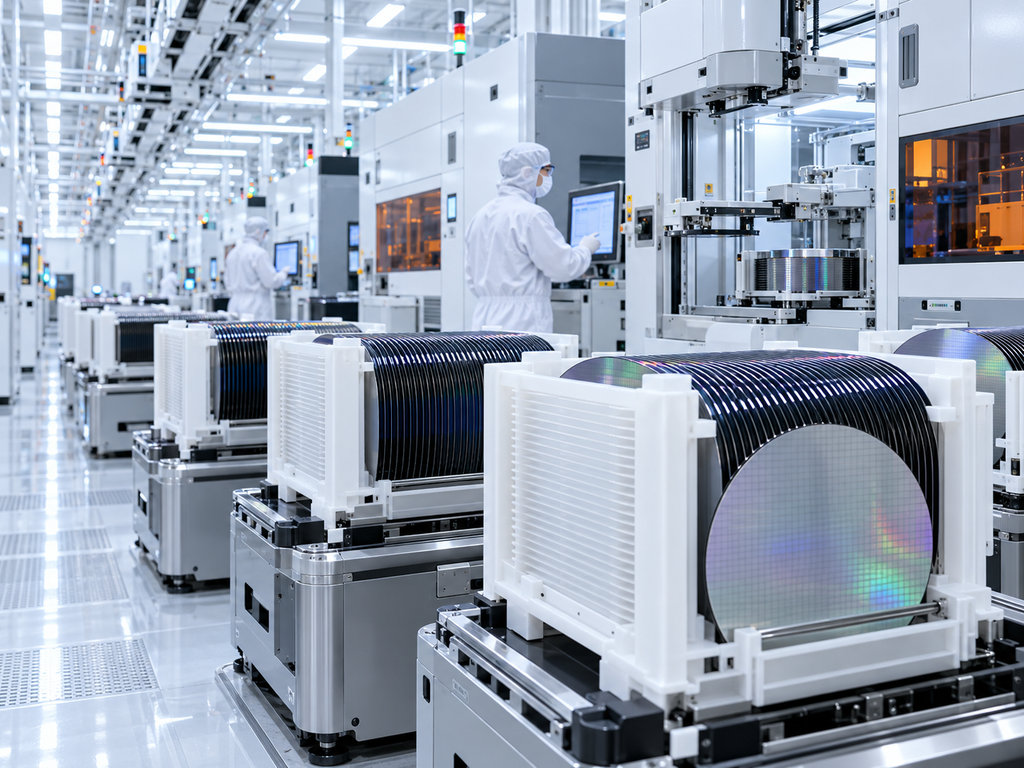
Why the Semiconductor Industry Continues Moving Toward 300mm
Larger wafers provide a major manufacturing advantage: more dies can be produced from each wafer.
Compared with 200mm manufacturing, a 300mm wafer offers significantly more usable surface area. Once a manufacturing process reaches sufficient volume, the larger format can improve productivity and reduce manufacturing cost per die.
For this reason, most leading-edge logic, DRAM, NAND and advanced semiconductor processes are based on 300mm infrastructure.
SEMI currently tracks hundreds of 300mm fabs and production lines worldwide, and additional facilities are continuing to move through construction and equipment installation.
The latest forecast indicates that this expansion is accelerating.
AI Is Reshaping Fab Investment
Artificial intelligence is one of the strongest forces behind the current investment cycle.
AI accelerators require advanced logic chips, while large AI systems also consume significant volumes of high-bandwidth memory.
SEMI reported separately that 300mm memory equipment investment was expected to exceed US$50 billion in 2026, supported by demand for HBM, DDR5 and data-center storage.
This creates investment across multiple parts of the semiconductor manufacturing chain:
- advanced logic;
- DRAM and HBM;
- NAND flash;
- advanced packaging;
- specialty semiconductor processes;
- wafer inspection and metrology.
Every new production line requires extensive equipment qualification before high-volume manufacturing begins.
That is where non-product wafers become essential.
What Is a Dummy Wafer?
A dummy wafer is a wafer used for semiconductor process support rather than for manufacturing saleable integrated circuits.
Dummy wafers can be used for:
- process chamber conditioning;
- equipment setup;
- temperature stabilization;
- thin-film deposition testing;
- etching tests;
- equipment calibration;
- contamination monitoring;
- process development;
- operator training.
In many applications, using production-grade device wafers would be unnecessarily expensive.
A suitable dummy wafer provides a stable and economical alternative.
Depending on the application, dummy wafers can be made from silicon, quartz, sapphire, SiC or other materials.
Silicon remains one of the most widely used options because it is compatible with standard semiconductor handling equipment.
Why New Fab Capacity Increases Dummy Wafer Demand
When a new semiconductor fab begins operating, production tools must undergo qualification before manufacturing valuable device wafers.
Consider a modern fab containing deposition, oxidation, diffusion, etching, ion implantation, cleaning and inspection systems.
Each tool may require multiple qualification runs.
Dummy wafers may be repeatedly used during:
Tool installation
Engineers verify mechanical handling, wafer transfer and chamber operation.
Process qualification
Engineers establish process windows and confirm repeatability.
Chamber seasoning
Some deposition and etch systems require conditioning before product wafers are introduced.
Preventive maintenance
After chamber cleaning or component replacement, dummy wafers can help confirm that the process has returned to stable conditions.
Process monitoring
Monitor wafers may be used periodically to track film thickness, particles, uniformity or other performance parameters.
As the number of 300mm tools increases, supporting wafer consumption can also increase.
300mm Wafers Create Stricter Handling Requirements
A 300mm silicon wafer is physically larger and heavier than smaller wafer formats, while modern automated fabs demand extremely precise handling.
Important wafer characteristics include:
- diameter tolerance;
- thickness;
- total thickness variation;
- bow;
- warp;
- edge profile;
- surface condition;
- particle cleanliness.
Even when a wafer is intended only for equipment qualification, poor geometry can cause handling problems.
For example, excessive wafer warp can interfere with robotic transfer or vacuum chucking. Incorrect edge geometry can affect alignment. Surface contamination can also influence process results.
For this reason, dummy wafers should be selected according to their actual process function rather than treated as simple low-cost silicon discs.
Dummy Wafers, Monitor Wafers and Test Wafers Are Not Always the Same
The terminology used across semiconductor fabs can vary.
A dummy wafer is generally used to support equipment operation or process conditioning.
A monitor wafer is more commonly used to measure process performance.
A test wafer may be used for R&D, equipment development or process experiments.
The required specification can therefore differ significantly.
A chamber-conditioning wafer may not need the same surface quality as a wafer used for particle measurement or thin-film uniformity testing.
Buyers should define the application before selecting:
- wafer grade;
- resistivity;
- crystal orientation;
- surface finish;
- thickness;
- edge type;
- cleanliness requirement.
This can prevent unnecessary cost while still meeting technical requirements.
Wafer Carriers Also Become More Important
More 300mm wafer production also means more wafer movement.
Wafers must travel between load ports, FOUPs, process chambers, inspection stations and other equipment.
During specialized operations such as thinning or advanced packaging, additional carrier wafers may also be required.
Carrier substrates must provide stable mechanical support and reliable geometry.
Typical requirements may include:
- low TTV;
- controlled bow and warp;
- polished surfaces;
- customized thickness;
- thermal stability;
- chemical resistance.
As semiconductor manufacturing becomes more automated, dimensional consistency becomes even more important.
What the 2026 Expansion Means for Material Suppliers
SEMI projects 20 new 300mm fabs or lines, excluding pure R&D facilities, to begin construction worldwide in 2026, followed by another 18 in 2027.
This does not mean all capacity will enter production immediately. Semiconductor fabs require long construction, installation and qualification cycles.
However, it indicates sustained demand for the broader semiconductor supply chain.
Material suppliers can expect increasing customer attention to:
- 300mm silicon wafers;
- dummy wafers;
- monitor wafers;
- carrier wafers;
- reclaimed wafers;
- process qualification substrates;
- wafer handling components.
Customers may also need relatively small quantities during equipment development before moving to regular production volumes.
Flexible supply capability can therefore be valuable.
Customized Wafer Specifications Are Becoming More Common
Not every process requires a standard prime-grade wafer.
Equipment manufacturers, universities, laboratories and semiconductor fabs may need custom specifications such as:
- unusual thicknesses;
- SSP or DSP surfaces;
- specific resistivity ranges;
- custom crystal orientations;
- oxide-coated wafers;
- patterned wafers;
- custom edge profiles;
- laser-marked wafers;
- small-batch quantities.
Understanding the intended process can help determine which specifications matter and which can be relaxed to reduce cost.
Looking Toward 2029
The current 300mm expansion cycle is not expected to end in 2026.
SEMI’s October outlook forecasts continued growth in 2027, 2028 and 2029, with global 300mm front-end equipment spending potentially reaching US$227 billion by 2029.
AI, advanced memory, high-performance computing and regional semiconductor supply-chain investment are all contributing to the trend.
As new manufacturing capacity comes online, the industry will need more than sophisticated lithography, deposition and etching tools.
Every production tool also depends on the materials used to install, qualify, monitor and maintain the process.
For this reason, dummy wafers, monitor wafers, carrier wafers and other semiconductor process-support substrates are likely to remain an important part of the 300mm manufacturing ecosystem.