
Artificial intelligence is changing not only chip architecture but also the way semiconductor devices are packaged. As AI accelerators, high-bandwidth memory (HBM), chiplets and 3D integrated circuits become more complex, advanced packaging is moving closer to the precision requirements traditionally associated with front-end wafer fabrication.
In October 2026, Applied Materials and BE Semiconductor Industries (Besi) announced an expansion of their strategic partnership focused on next-generation 3D IC integration, hybrid bonding, thermo-compression bonding and new die-to-wafer and die-to-die architectures. The development reflects a broader industry trend: packaging is increasingly becoming a critical part of semiconductor performance scaling rather than simply the final assembly stage.
For semiconductor manufacturers, this shift is creating new requirements for wafer thinning, temporary wafer bonding, carrier wafers, surface preparation and ultra-precise wafer handling.
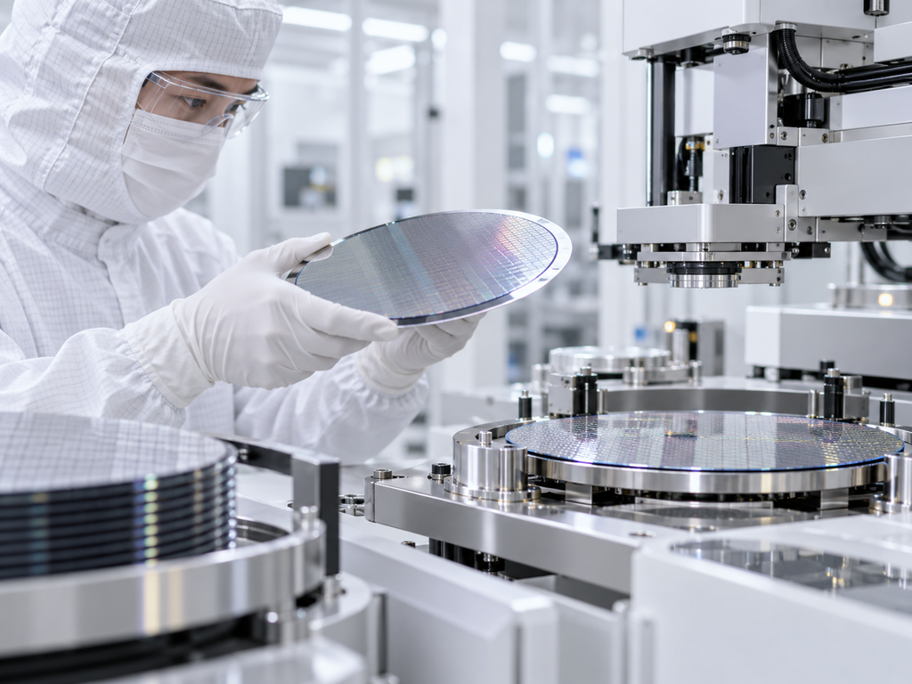
Why AI Chips Are Driving Thinner Wafers
Traditional semiconductor packages could tolerate relatively thick silicon wafers during much of the manufacturing process. Advanced 2.5D and 3D packages are different.
To reduce package thickness and shorten electrical interconnect distances, wafers may need to be thinned significantly before stacking or bonding. In applications such as HBM and 3D integration, controlling the final wafer thickness becomes increasingly important.
A typical process may involve:
- temporary bonding of the device wafer to a carrier wafer;
- backside grinding and wafer thinning;
- stress-relief or polishing processes;
- backside metallization or redistribution processes;
- debonding;
- wafer or die inspection;
- hybrid bonding or subsequent package assembly.
As the wafer becomes thinner, its mechanical strength decreases. Bow, warp, cracking and edge damage become more difficult to control.
This is where the temporary wafer carrier becomes important.
The Role of Temporary Wafer Carriers
A temporary wafer carrier provides mechanical support while a semiconductor wafer undergoes thinning and backside processing.
The carrier must remain dimensionally stable through multiple process steps while maintaining compatibility with bonding and debonding systems.
Depending on the process, carrier materials may include silicon, glass, sapphire or other engineered substrates. Material selection depends on factors such as thermal expansion, thermal stability, transparency requirements, chemical compatibility and equipment configuration.
Important carrier wafer specifications can include:
Diameter and thickness tolerance
The carrier must be compatible with standard wafer-processing equipment and maintain stable geometry during bonding.
Total thickness variation
Low TTV helps support uniform grinding and reduces non-uniform pressure across the bonded wafer pair.
Bow and warp
Excessive deformation can create problems during chucking, grinding, lithography, bonding and automated wafer handling.
Surface flatness and roughness
The bonding interface must support uniform contact and controlled adhesive thickness.
Edge profile
Edge geometry can influence bonding quality and mechanical stability, particularly during high-speed grinding.
These requirements become more challenging as advanced packaging moves toward larger wafers and increasingly thin device layers.
Wafer Thinning Is Becoming a Precision Process
Wafer thinning may sound relatively straightforward, but removing hundreds of micrometers of silicon while maintaining micron-level thickness control is a highly demanding process.
Back grinding typically removes most of the bulk material. Additional fine grinding, polishing or stress-relief processes may then be used to reduce subsurface damage.
Several parameters must be controlled simultaneously:
- final wafer thickness;
- total thickness variation;
- backside roughness;
- edge chipping;
- bow and warp;
- residual stress;
- particle contamination.
For very thin wafers, even small variations in grinding pressure or carrier flatness can influence final wafer geometry.
The growth of AI packaging therefore increases demand not only for advanced bonding equipment but also for precision wafer substrates, carrier wafers and supporting materials used throughout the thinning process.
Hybrid Bonding Changes Surface Requirements
Hybrid bonding is one of the most important technologies in next-generation advanced packaging.
Unlike conventional solder-based interconnects, hybrid bonding can create direct dielectric and metal-to-metal connections at extremely fine pitches. This can significantly increase interconnect density while reducing electrical resistance and power consumption.
However, the technology places much stricter requirements on surface preparation.
Particles, local surface defects, wafer bow or non-uniform topography can lead to bonding voids or poor interconnect formation.
Important factors include:
- surface cleanliness;
- nanometer-scale roughness;
- wafer flatness;
- copper surface preparation;
- alignment accuracy;
- particle control;
- bonding temperature and pressure.
As pitch sizes decrease, these requirements become even tighter.
This is one reason advanced packaging increasingly resembles front-end semiconductor manufacturing.
Wafer Handling Becomes More Difficult After Thinning
Automated semiconductor equipment is generally designed around predictable wafer geometry and stiffness.
Once a wafer becomes extremely thin, conventional handling methods become more difficult.
Thin wafers can flex during transfer. Vacuum pressure that is safe for a standard wafer may deform a thin wafer. Contact points can introduce local stress.
Temporary carriers help maintain compatibility with existing wafer-processing infrastructure.
Carrier wafers can allow fragile device wafers to continue moving through:
- robotic wafer transfer systems;
- vacuum chucks;
- grinding equipment;
- coating systems;
- cleaning equipment;
- inspection tools;
- bonding equipment.
The dimensional quality of the carrier therefore becomes part of overall process stability.
HBM and 3D ICs Increase the Importance of Yield
Advanced AI packages can contain multiple high-value dies and memory stacks.
This changes the economics of packaging.
A defect introduced late in the process can affect an assembly containing multiple expensive semiconductor components. As a result, process stability, contamination control and wafer handling become increasingly important.
Manufacturers are therefore paying greater attention to seemingly simple components such as:
- carrier wafers;
- dummy wafers;
- process test wafers;
- grinding support substrates;
- precision wafer holders;
- bonding substrates.
These materials may not perform the computing function of the final chip, but they can directly influence manufacturing yield.
From Die-to-Wafer to Die-to-Die Integration
The advanced packaging roadmap is also becoming more diverse.
Applied Materials and Besi have indicated that development is expanding beyond traditional die-to-wafer hybrid bonding toward die-to-die, die-to-panel and other integration architectures.
This means semiconductor manufacturers will need flexible materials and handling strategies capable of supporting multiple packaging platforms.
Large package sizes, increasingly dense interconnects and thinner semiconductor layers will make dimensional control even more important.
What This Means for Semiconductor Material Suppliers
For suppliers of semiconductor wafers and precision substrates, advanced packaging represents an expanding technical market.
Customers increasingly require customized wafer specifications rather than standard catalog products.
Typical requirements may include:
- 100 mm, 150 mm, 200 mm or 300 mm diameter;
- customized carrier wafer thickness;
- SSP or DSP surfaces;
- controlled TTV;
- low bow and warp;
- custom edge profiles;
- surface polishing;
- laser marking;
- customized resistivity or crystal orientation;
- small quantities for R&D and larger batches for production.
The ability to provide technical drawings, inspection data and consistent batch-to-batch quality is becoming increasingly important.
Looking Ahead
AI is pushing semiconductor scaling beyond individual transistor dimensions.
The next generation of performance improvements will increasingly depend on how logic, memory and other functional dies are integrated inside a package.
As hybrid bonding, HBM and 3D IC technologies move toward higher-volume production, wafer thinning and temporary bonding will become even more important.
That creates new opportunities for precision carrier wafers, dummy wafers, semiconductor substrates and wafer-processing materials.
Advanced packaging may take place at the end of the semiconductor manufacturing flow, but the precision it requires is increasingly comparable to the front end of the fab.
For semiconductor material suppliers, understanding this transition will be essential to supporting the next generation of AI hardware.