
As advanced semiconductor processes continue to scale, silicon wafer specifications are becoming increasingly application-specific.
For certain advanced logic, CMOS image sensor, analog, power and specialty semiconductor processes, a standard polished silicon wafer may not provide the required surface-layer electrical properties or crystalline quality.
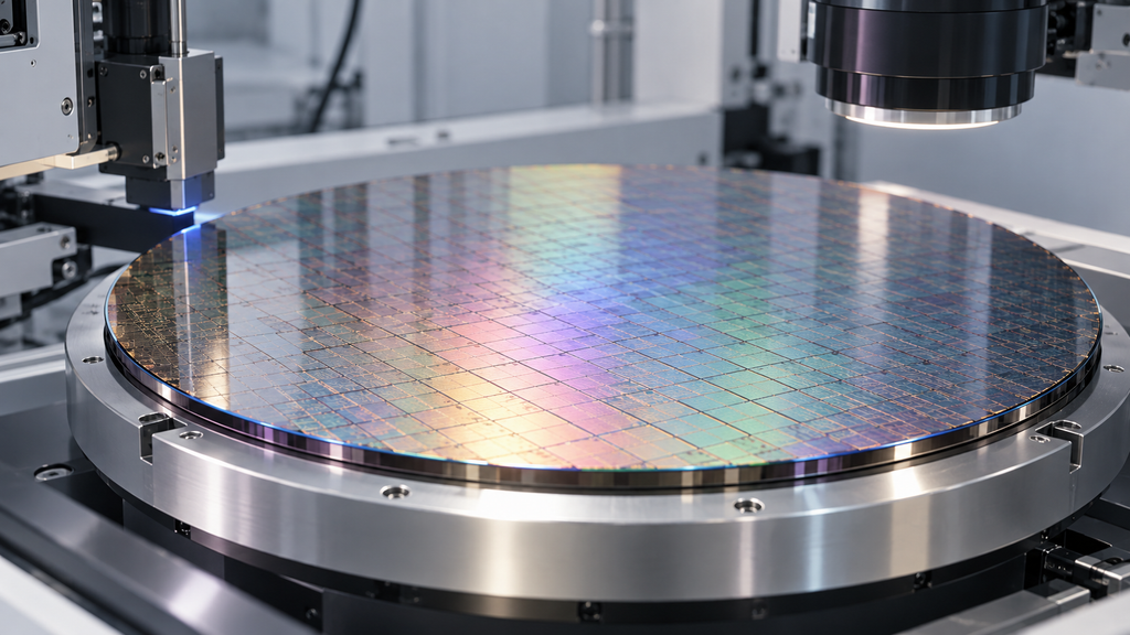
An epitaxial silicon wafer provides another option.
Instead of fabricating devices directly on the polished bulk silicon surface, a controlled layer of single-crystal silicon is grown epitaxially on the substrate.
This allows wafer manufacturers and device engineers to independently control important characteristics such as:
- Epitaxial layer thickness
- Epitaxial resistivity
- Dopant type and concentration
- Surface crystal quality
- Defect density
- Wafer flatness
- Edge condition
- Particle level
- Surface roughness
For 300mm wafers used in demanding semiconductor processes, controlling these parameters consistently across the entire wafer becomes especially important.
This article examines the most important specifications engineers should consider when selecting or qualifying 300mm epitaxial silicon wafers.
1. What Is a 300mm Epitaxial Silicon Wafer?
An epitaxial silicon wafer normally begins with a polished monocrystalline silicon substrate.
A thin layer of single-crystal silicon is then grown on the polished surface using an epitaxial deposition process.
A simplified structure is:
Epitaxial Silicon Layer
↓
Interface
↓
Bulk Silicon Substrate
The epitaxial layer maintains the crystallographic relationship of the underlying silicon substrate.
Unlike a deposited amorphous or polycrystalline film, the epi layer continues the single-crystal structure of the wafer.
The substrate and epitaxial layer can also be engineered with different electrical properties.
For example:
Low-resistivity substrate + higher-resistivity epi layer
or
Higher-resistivity substrate + controlled doped epi layer
depending on the device architecture.
This ability to independently engineer the surface layer is one of the primary reasons epitaxial wafers are used.
2. Why Use Epitaxial Silicon Instead of a Standard Polished Wafer?
A polished silicon wafer already provides a high-quality single-crystal surface.
So why add an epitaxial layer?
The answer depends on device requirements.
An epitaxial layer can provide several advantages.
Controlled Surface Resistivity
The electrical properties of the device-forming region can be engineered separately from the bulk substrate.
Improved Surface Crystal Quality
The active device region can be grown under tightly controlled conditions.
Dopant Profile Control
The dopant concentration of the epi layer can differ significantly from the underlying substrate.
Device Isolation
Certain device structures benefit from a controlled epitaxial layer above a more heavily doped substrate.
Defect Engineering
The relationship between substrate defects, oxygen concentration, gettering behavior and the device-active region can be optimized for the process.
However, epi wafers also add complexity and cost.
They should therefore be specified when the device process requires the additional electrical or crystalline control rather than simply because epitaxial wafers are considered “higher grade.”
3. Epitaxial Layer Thickness
Epi thickness is one of the first specifications that must be defined.
Depending on the application, the layer may range from relatively thin films to substantially thicker epitaxial structures.
There is no universal thickness for a 300mm logic epi wafer.
The required thickness depends on:
- Device architecture
- Junction depth
- Implantation process
- Isolation structure
- Electrical breakdown requirement
- Thermal process
- Subsequent material removal
- Device-generation requirements
Therefore, a purchasing specification should not simply state:
300mm Epitaxial Silicon Wafer
It should specify the required epitaxial thickness and tolerance.
For example:
Epi thickness: Target ± tolerance
The exact values should be determined by the process design.
4. Why Epi Thickness Uniformity Matters
Average epi thickness alone is not enough.
Uniformity across the 300mm wafer is often equally important.
If the epitaxial layer is thicker near one region and thinner in another, subsequent device processes may behave differently across the wafer.
Potential consequences include variation in:
- Junction characteristics
- Electrical resistance
- Implantation response
- Device performance
- Process window
- Yield
Thickness uniformity can be described using several methods.
For example:
- Maximum-minimum variation
- Percentage nonuniformity
- Center-to-edge variation
- Site-based mapping
- Edge-excluded mapping
When comparing suppliers, engineers should confirm that both sides are using the same measurement methodology.
Two wafers can appear to have different “uniformity” values simply because different edge exclusions or calculation methods were used.
5. Epitaxial Resistivity
Resistivity is another critical parameter.
Silicon resistivity is closely related to dopant type and concentration.
Common dopants include:
P-Type
Typically associated with acceptor dopants such as boron.
N-Type
Typically associated with donor dopants such as phosphorus, arsenic or antimony, depending on the required structure and manufacturing process.
For an epitaxial wafer, engineers may need to specify separately:
Substrate conductivity type
Substrate resistivity
Epitaxial conductivity type
Epitaxial resistivity
These should not be treated as one parameter.
For example, two wafers can have identical dimensions and epi thickness but completely different electrical structures.
6. Resistivity Uniformity Across a 300mm Wafer
For advanced semiconductor processing, the nominal resistivity value is only part of the specification.
Across-wafer uniformity also matters.
During epitaxial growth, dopant incorporation must remain controlled across the wafer surface.
Nonuniform resistivity can produce variations in electrical device characteristics.
Engineers may therefore request:
- Center resistivity
- Mean resistivity
- Radial mapping
- Within-wafer variation
- Lot-to-lot consistency
Measurement method should also be specified where necessary.
This becomes particularly important when comparing qualification data from different wafer suppliers.
7. Substrate Resistivity and Epi Resistivity Should Not Be Confused
This is a common mistake when requesting epitaxial silicon wafers.
Consider a wafer with:
Substrate: P-type, low resistivity
and
Epi layer: P-type, higher resistivity
The finished wafer does not have one single meaningful resistivity value for every engineering purpose.
The substrate and epi layer perform different functions.
Therefore, an RFQ should clearly separate:
| Parameter | Requirement |
|---|---|
| Substrate type | P / N |
| Substrate dopant | Specify if required |
| Substrate resistivity | Ω·cm |
| Epi type | P / N |
| Epi dopant | Specify if required |
| Epi resistivity | Ω·cm |
| Epi thickness | µm |
This eliminates a significant source of specification ambiguity.
8. Defect Density in Epitaxial Silicon
For advanced device manufacturing, defect control is extremely important.
A defect in the active device region can influence:
- Leakage
- Breakdown behavior
- Junction performance
- Reliability
- Device yield
Epitaxial wafer inspection may therefore evaluate several categories of defects.
These can include:
- Epitaxial stacking faults
- Slip
- Surface particles
- Haze
- Pits
- Protrusions
- Crystallographic defects
- Localized growth defects
- Contamination-related defects
Not every defect has the same electrical impact.
For this reason, engineers should avoid using a vague specification such as:
“Low defect density required.”
Instead, the defect class, detection threshold and allowable count should be defined whenever the application requires it.
9. Epitaxial Stacking Faults
Epitaxial stacking faults are one defect category that may occur during silicon epitaxial growth.
Their formation can be related to factors including:
- Substrate surface condition
- Particles
- Surface contamination
- Crystal defects
- Epitaxial growth conditions
Because an epitaxial defect can propagate through the grown layer, the incoming substrate surface and epitaxial reactor cleanliness are both important.
For sensitive applications, defect maps may be more useful than a simple total defect count.
A map can reveal whether defects are:
- Random
- Edge concentrated
- Center concentrated
- Patterned
- Associated with handling
This can provide important information during root-cause analysis.
10. Particle Specifications
Particles are another major concern.
As device geometries become smaller, the minimum particle size included in wafer inspection specifications can become increasingly demanding.
A useful particle specification should define:
Particle size threshold + maximum count + inspection area
For example, merely saying:
Particles < 10
is incomplete.
Ten particles above what size?
Across the entire wafer or inside a specific edge exclusion?
Measured using which inspection tool?
These details matter when qualifying high-quality 300mm wafers.
11. Surface Roughness
The epitaxial surface should provide a high-quality starting surface for subsequent semiconductor processing.
Surface roughness may influence:
- Gate stack preparation
- Oxidation
- Thin-film deposition
- Lithography
- Bonding
- Interface quality
Atomic force microscopy may be used when very low surface roughness must be characterized.
Depending on the application, the specification may include:
- Ra
- RMS roughness
- Scan size
- Measurement location
A roughness value without a scan area or measurement method can be difficult to compare across suppliers.
12. 300mm Wafer Geometry
For advanced semiconductor fabrication, epi electrical properties alone are not enough.
The physical wafer geometry must also be tightly controlled.
Important parameters include:
- Diameter
- Thickness
- TTV
- Bow
- Warp
- Global flatness
- Local flatness
- Site flatness
- Edge profile
These parameters become especially important during lithography, inspection and precision wafer handling.
13. TTV, Bow and Warp Are Different Parameters
These terms are sometimes incorrectly used interchangeably.
TTV — Total Thickness Variation
TTV describes the difference between the maximum and minimum wafer thickness.
It is fundamentally a thickness-uniformity measurement.
Bow
Bow describes the displacement of the wafer center relative to a reference plane under specified measurement conditions.
Warp
Warp describes the overall deviation of the wafer from a reference plane and captures more complex wafer deformation.
A wafer may have low TTV but still show significant bow.
Likewise, wafer stress introduced during epitaxial growth can affect bow or warp without necessarily producing large thickness variation.
Therefore, all three parameters may need to be controlled separately.
14. Why Flatness Is Particularly Important for Advanced Logic
Modern lithography operates with increasingly demanding focus budgets.
If a wafer surface moves vertically outside the allowable process window, lithographic focus can be affected.
Wafer flatness therefore influences:
- Exposure focus
- Overlay
- CD control
- Process uniformity
- Yield
The effect is especially important when device features occupy increasingly small dimensions.
For this reason, advanced wafer qualification typically goes beyond simple global wafer thickness.
Local site flatness can become critical.
15. Edge Specifications Are Often Overlooked
Many wafer RFQs carefully specify:
- Diameter
- Thickness
- Resistivity
- Orientation
- Surface roughness
but leave the wafer edge almost undefined.
For modern automated fabs, this can be a mistake.
The edge participates directly in:
- Robotic handling
- Edge gripping
- Alignment
- Edge inspection
- Lithography edge exclusion
- Film deposition
- Cleaning
- Wafer chucking
The edge should therefore be treated as an engineered area.
16. Wafer Edge Profile
The edge of a silicon wafer is normally shaped rather than left sharp.
A controlled edge profile helps reduce mechanical damage and improves wafer handling.
Important edge characteristics may include:
- Bevel geometry
- Edge radius
- Edge symmetry
- Edge roughness
- Chips
- Cracks
- Edge damage
- Polishing quality
An incorrectly processed wafer edge can become a source of particles or fracture initiation.
This becomes particularly important in high-speed automated 300mm handling systems.
17. Edge Exclusion
Many wafer measurements intentionally exclude a narrow region near the wafer perimeter.
This is called edge exclusion.
For example, a flatness or particle measurement may be reported over:
300mm wafer minus defined edge exclusion
The exact exclusion depends on:
- Measurement standard
- Customer specification
- Device layout
- Process equipment
- Lithography requirements
It is critical that supplier and buyer use the same definition.
For example:
TTV ≤ X µm
means little unless measurement area and edge exclusion are understood.
This same principle applies to:
- Epi thickness uniformity
- Resistivity uniformity
- Surface defects
- Particles
- Flatness
18. Epi Edge Crown and Edge-Related Growth Effects
Epitaxial deposition near the wafer edge can behave differently from deposition across the central region.
Gas flow, thermal gradients and reactor geometry can create localized thickness variation.
Depending on the growth process, engineers may observe edge-related features such as:
- Increased thickness
- Reduced thickness
- Local surface morphology variation
- Edge crown
These effects must remain outside the active process area or within the customer-defined specification.
The relationship between:
epitaxial growth profile
and
device edge exclusion
should therefore be considered during wafer qualification.
19. Crystal Orientation
Crystal orientation is another fundamental wafer parameter.
Common silicon orientations include:
- (100)
- (111)
- Other application-specific orientations
Advanced logic commonly uses carefully controlled crystallographic orientation because device performance and process behavior depend on the silicon crystal plane.
Orientation specifications may also include:
- Surface orientation
- Off-angle
- Orientation tolerance
- Notch direction
A purchase specification should not simply state “single-crystal silicon.”
20. Notch Geometry and Automated Handling
300mm wafers typically use a notch for orientation identification.
The notch supports:
- Wafer alignment
- Crystal orientation identification
- Robotic handling
- Process tracking
For automated equipment, notch position and geometry must remain compatible with:
- Pre-aligners
- Load ports
- Robot end effectors
- Inspection systems
- Process stages
The wafer edge is therefore both a material specification and an equipment-interface specification.
21. Surface Metal Contamination
Ultra-clean silicon surfaces are required for advanced semiconductor fabrication.
Metal contamination such as:
- Fe
- Cu
- Ni
- Cr
- Na
- K
can negatively affect device performance even at very low concentrations.
Wafer manufacturing and epitaxial processes therefore require strict contamination control.
Possible sources include:
- Reactor components
- Process gases
- Wet chemistry
- Handling tools
- Cleaning systems
- Packaging
- Human handling
For critical applications, customers may request surface metal analysis as part of wafer qualification.
22. Packaging Is Part of the Wafer Specification
A high-quality wafer can still arrive contaminated or damaged if packaging is poorly controlled.
300mm epi wafers may be supplied using semiconductor-compatible wafer carriers or shipping systems designed to protect:
- Front surface
- Back surface
- Wafer edge
- Notch area
Packaging requirements may include:
- Cleanroom packing
- Double bagging
- Nitrogen environment
- Controlled particle level
- Lot traceability
- Individual wafer identification
Packaging should therefore be included in supplier qualification rather than treated as a separate logistics issue.
23. Lot-to-Lot Consistency
For development projects, one excellent wafer lot is not enough.
Production requires consistency.
Important lot-to-lot parameters can include:
- Epi thickness
- Thickness uniformity
- Epi resistivity
- Resistivity uniformity
- Particle level
- Defect density
- TTV
- Bow
- Warp
- Surface metals
A supplier may meet every individual specification yet still create process problems if parameters consistently shift from lot to lot within the allowed tolerance window.
For advanced semiconductor processes, statistical consistency is often as important as the nominal specification.
24. What Should Be Included in a 300mm Epitaxial Wafer RFQ?
A detailed RFQ greatly reduces communication errors.
A typical engineering specification may include:
| Parameter | Example Information to Specify |
|---|---|
| Diameter | 300 mm |
| Crystal growth | CZ / application-specific |
| Crystal orientation | (100), etc. |
| Conductivity | P-type / N-type |
| Substrate dopant | B / P / As / Sb if required |
| Substrate resistivity | Target range |
| Epi conductivity | P / N |
| Epi dopant | Specify where required |
| Epi resistivity | Target range |
| Epi thickness | Target ± tolerance |
| Epi uniformity | Maximum variation |
| Wafer thickness | Target ± tolerance |
| TTV | Maximum |
| Bow | Maximum |
| Warp | Maximum |
| Surface roughness | Ra/RMS + scan condition |
| Particle specification | Size threshold + maximum count |
| Epi defects | Type and maximum count |
| Edge exclusion | Defined measurement area |
| Edge profile | Required standard/profile |
| Surface | Epi front / polished backside |
| Notch | Orientation and specification |
| Metal contamination | Limits if required |
| Packaging | 300mm carrier / clean packaging |
| Quantity | Sample / qualification / production |
25. Example RFQ Format
A purchasing inquiry should ideally look something like this:
Product: 300mm Epitaxial Silicon Wafer
Diameter: 300mm
Orientation: (100)
Substrate Type: P-type
Substrate Resistivity: Customer specified
Epi Type: P-type
Epi Thickness: Customer specified
Epi Thickness Tolerance: Customer specified
Epi Resistivity: Customer specified
TTV: Customer specified
Bow: Customer specified
Warp: Customer specified
Surface: Epi front surface
Defect Requirement: Customer specified
Particle Requirement: Size threshold and count required
Edge Exclusion: Customer specified
Quantity: Qualification samples followed by production volume
This is considerably more useful than simply requesting:
“Please quote 300mm epi silicon wafers.”
26. Questions to Ask a 300mm Epitaxial Wafer Supplier
Before qualification, semiconductor buyers should consider asking:
- What epi thickness range can be controlled?
- What thickness-uniformity method is used?
- How is epi resistivity measured?
- What resistivity uniformity can be provided?
- How are epi defects classified?
- What particle-size threshold is used for inspection?
- What edge exclusion is applied to inspection data?
- What TTV, bow and warp levels can be supported?
- What edge profile is supplied?
- What surface-metal contamination data can be provided?
- Can wafer maps be supplied?
- Is lot-level traceability available?
- Can sample wafers be provided for process qualification?
- What parameters are included on the certificate of analysis?
- Can specifications be customized for production orders?
The answers to these questions are often more important than unit price during the initial qualification stage.
Conclusion
A 300mm epitaxial silicon wafer should not be evaluated by diameter and resistivity alone.
For demanding semiconductor applications, the complete specification includes:
Epi thickness + epi resistivity + dopant profile + defect density + particle level + surface quality + wafer geometry + edge condition
These parameters interact with one another.
Epitaxial thickness affects the device structure.
Resistivity determines the electrical properties of the active layer.
Defects and contamination influence yield and reliability.
TTV, bow, warp and local flatness affect lithography and wafer handling.
Edge geometry and edge exclusion influence both inspection results and compatibility with automated equipment.
For engineers sourcing 300mm epitaxial silicon wafers, the most effective approach is therefore to define the device and process requirements first, then translate those requirements into measurable wafer specifications.
A detailed RFQ and clear qualification criteria can significantly reduce the risk of receiving wafers that meet a general datasheet but do not meet the actual process window.