
Wafer-level metal plating has become an important process in both semiconductor fabrication and advanced packaging.
Applications range from redistribution layers and copper pillars to TSV filling, under-bump metallization, backside electrodes and high-current metallization structures.
As feature dimensions become smaller and wafers become larger, however, simply depositing metal is no longer enough.
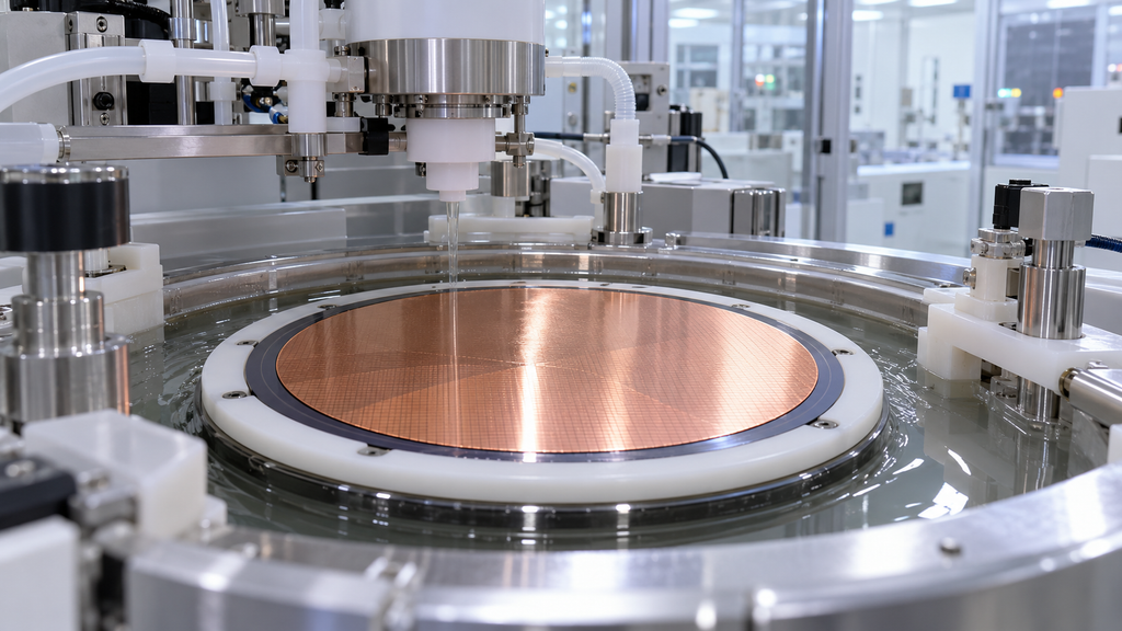
Manufacturers must control:
- Seed layer continuity
- Sheet resistance
- Plating thickness uniformity
- Edge current density
- Wafer edge exclusion
- Metal adhesion
- Backside contamination
- Wafer bow and stress
- Surface roughness
- Post-plating reliability
A plating process that performs well at the center of a wafer may behave very differently close to the edge.
Likewise, a seed layer that appears acceptable on a blanket wafer may produce poor filling when used inside high-aspect-ratio structures.
For this reason, wafer plating should be treated as a complete process integration problem rather than an isolated deposition step.
1. Where Wafer Plating Is Used in Semiconductor Manufacturing
Electrochemical deposition, commonly called electroplating, is widely used because relatively thick metal layers can be deposited efficiently while maintaining good electrical conductivity.
Typical wafer-level applications include:
- Copper redistribution layers
- Cu pillars
- Micro-bumps
- TSV metallization
- TGV metallization
- Under-bump metallization
- Backside metal electrodes
- Power-device metallization
- MEMS structures
- RF devices
- Thermal-management structures
- Wafer-level packaging
Copper is one of the most important electroplated metals because of its high electrical and thermal conductivity.
Depending on the application, other deposited metals may include:
- Nickel
- Gold
- Silver
- Tin
- Cu/Sn structures
- Ni/Au systems
- Ni/Pd/Au systems
The optimum metal system depends on the electrical, bonding, soldering, thermal and reliability requirements of the final device.
2. Why the Seed Layer Is Critical
Electroplating requires an electrically conductive surface.
For many semiconductor processes, a thin conductive seed layer is deposited before electroplating. Copper seed layers are commonly used for copper electroplating, often together with an adhesion or diffusion-barrier layer.
A simplified structure may look like:
Silicon / Dielectric / Barrier / Cu Seed / Electroplated Cu
The exact stack depends on the device.
The seed layer performs several important functions:
- Provides an electrical path across the wafer
- Allows current to reach the plating area
- Provides nucleation sites for deposited metal
- Influences adhesion
- Influences initial grain growth
- Affects final plating uniformity
Therefore, seed layer quality directly affects the subsequent plating result.
Seed Layer Thickness
A seed layer that is too thin may have excessive sheet resistance.
Since electrical contact to the wafer is often made near the perimeter, current must travel through the conductive seed layer toward other areas of the wafer.
If resistance is too high, the local electrical potential can vary across the wafer.
This can create:
- Center-to-edge thickness variation
- Slow deposition in high-resistance areas
- Poor feature filling
- Local plating defects
However, simply making the seed layer thicker is not always the solution.
Thicker seed layers may affect:
- Fine-line dimensions
- Seed removal
- Critical dimensions
- Cost
- Process integration
The target should therefore be sufficient conductivity combined with controlled thickness.
3. Seed Layer Uniformity Means More Than Average Thickness
When engineers discuss seed uniformity, they should consider several parameters.
Thickness Uniformity
The deposited film should remain within the required thickness window across the wafer.
Large thickness variation can produce different local current densities during electroplating.
Continuity
A seed layer may have an acceptable average thickness but still contain discontinuities.
This is particularly important in:
- Deep vias
- High-aspect-ratio features
- Vertical sidewalls
- Re-entrant structures
A discontinuous seed layer can interrupt the electrical path and lead to incomplete filling.
Step Coverage
For TSV or similar structures, depositing metal on the wafer surface is relatively easy.
Depositing a continuous seed layer along the entire sidewall and near the bottom of a deep feature is much more difficult.
Poor step coverage can result in:
- Voids
- Seam formation
- Incomplete filling
- High electrical resistance
- Reliability failure
Sheet Resistance
Four-point probe measurements can be used to evaluate sheet resistance across blanket seed wafers.
A sheet-resistance map can reveal radial or localized nonuniformity that may later appear as plating nonuniformity.
Surface Condition
Seed-layer surface conditions can influence metal nucleation.
Important factors include:
- Oxidation
- Surface contamination
- Roughness
- Native oxide
- Time between seed deposition and plating
For copper seed layers, excessive surface oxidation before plating can negatively influence adhesion and deposition behavior.
4. Why Wafer Edge Plating Is Difficult
The wafer edge is one of the most challenging areas in electroplating.
Electrical current distribution near the perimeter is naturally different from that in the central region.
This can create a phenomenon commonly associated with increased local current density near the wafer edge.
The result may be:
Center
Relatively stable deposition
Edge
Higher deposition rate or localized over-plating
Without sufficient process control, this can cause a radial thickness profile such as:
thin → nominal → increasingly thick near the wafer edge
For advanced packaging, even relatively small height differences can become important.
For example, excessive thickness variation in Cu pillars can influence:
- Coplanarity
- Bonding
- Assembly yield
- Mechanical stress
- Electrical reliability
5. What Is Wafer Edge Exclusion?
Edge exclusion refers to a controlled region near the perimeter of the wafer that is intentionally kept outside the active processing area or treated differently from the main wafer surface.
In plating processes, edge exclusion serves several functions.
It can help prevent:
- Metal deposition on the bevel
- Uncontrolled edge plating
- Chemical leakage around the wafer seal
- Metal contamination on the backside
- Electrical shorting to equipment components
- Edge flaking
- Particle generation
The required exclusion width is process-specific.
There is no single edge-exclusion value suitable for every wafer or plating system.
It depends on factors including:
- Wafer diameter
- Equipment design
- Electrical contact method
- Seal geometry
- Device layout
- Bevel geometry
- Downstream processing requirements
6. Wafer Edge Exposure and Edge Protection
Several process strategies can be used to control the wafer perimeter.
Depending on the process flow, these may include:
Wafer Edge Exposure
Lithography can be used to remove photoresist from selected areas near the wafer perimeter.
This can provide access for electrical contact or define the area that will not contain plated structures.
Edge Protection
Other regions may remain protected by resist or equipment sealing structures.
The objective is to prevent uncontrolled chemical or metal deposition.
Edge Bead Removal
Photoresist deposition often produces a thicker bead near the wafer edge.
Removing this bead improves subsequent process uniformity and reduces contamination risks.
Mechanical Sealing
Some plating equipment uses a seal close to the wafer perimeter.
The seal prevents electrolyte from reaching the wafer backside while allowing electrical contact with the seed layer.
Seal condition and placement are therefore important equipment parameters.
7. Controlling Across-Wafer Plating Uniformity
Plating uniformity is influenced by much more than seed-layer thickness.
Several variables interact simultaneously.
Current Density
According to Faraday’s law, deposited metal thickness is closely related to local current density and plating time.
If current density is nonuniform, deposition thickness will also tend to be nonuniform.
Wafer Rotation
Rotation can improve mass transport and reduce directional differences caused by fluid flow.
However, rotation alone cannot eliminate every electrical-field nonuniformity.
Electrolyte Flow
Flow influences the supply of metal ions and additives to the wafer surface.
Poor flow distribution can produce localized variations in plating rate.
Anode Geometry
The position and shape of the anode influence electrical-field distribution.
Equipment may use shields, auxiliary electrodes or other current-shaping methods to improve center-to-edge uniformity.
Pattern Density
A wafer containing dense metal features in one region and sparse features in another may plate differently from a blanket wafer.
Pattern-dependent plating becomes particularly important for:
- RDL
- Cu pillars
- Micro-bumps
- Large chiplets
- Heterogeneous layouts
Therefore, blanket-wafer uniformity data alone may not fully predict patterned-wafer performance.
8. Electrolyte Chemistry Also Controls the Deposit
Modern copper plating chemistry is not simply copper salt dissolved in water.
Typical systems may contain:
- Copper ions
- Acid
- Chloride
- Accelerator
- Suppressor
- Leveler
These additives control how quickly copper deposits at different locations.
The balance between accelerator, suppressor and leveler becomes particularly important in high-aspect-ratio filling.
A poorly controlled chemistry can lead to:
- Voids
- Seams
- Nodules
- Rough deposits
- Excessive edge deposition
- Nonuniform feature heights
Bath age and contamination also matter.
Production processes therefore often monitor:
- Metal concentration
- Acid concentration
- Chloride concentration
- Organic additives
- Temperature
- Conductivity
- Contamination
9. Pulse Plating and Advanced Current Control
Traditional plating commonly uses direct current.
More advanced processes may use:
- Pulse plating
- Pulse-reverse plating
- Variable-current recipes
- Multi-step current profiles
These techniques can help improve mass transport, feature filling and deposit properties.
For high-aspect-ratio structures, process engineers may intentionally change the current density during different stages of the fill.
The goal is often to encourage bottom-up deposition while avoiding premature closure near the top of the feature.
10. Backside Metallization Is Becoming More Important
Historically, many semiconductor processes concentrated most complex metal routing on the front side of the wafer.
However, wafer backside processing now plays a growing role in several device categories.
Examples include:
- Power semiconductors
- SiC devices
- Discrete devices
- MEMS
- Sensors
- RF devices
- Backside power delivery
- Advanced 3D integration
Backside metal may serve different purposes depending on the device.
These include:
- Electrical contact
- Power delivery
- Ground connection
- Die attach
- Soldering
- Thermal conduction
- Reflective layers
- Bonding surfaces
11. Typical Backside Metal Stacks
There is no universal backside metallization stack.
Different devices can require very different materials.
Possible metal systems may contain combinations of:
- Al
- Ti
- Cr
- Ni
- Cu
- Ag
- Au
- Pt
A simplified example might include:
Wafer → Adhesion Layer → Barrier Layer → Conductive Metal → Bonding/Protection Layer
For another device, the structure may be completely different.
When selecting a stack, engineers should consider:
Contact Resistance
The metal must form a sufficiently low-resistance electrical contact.
Adhesion
The metal stack must remain attached during subsequent thermal and mechanical processing.
Diffusion
A barrier layer may be required to prevent undesirable interdiffusion.
Solderability
Power-device backside contacts may need to be compatible with solder or sintered attach materials.
Oxidation Resistance
Some exposed metals require a protective finish.
Thermal Budget
Annealing steps must remain compatible with the device and frontside structures.
12. Backside Metallization After Wafer Thinning
Backside metallization often occurs after the wafer has been thinned.
A typical process sequence may involve:
Frontside protection
↓
Wafer grinding
↓
Stress relief / polishing / etching
↓
Backside cleaning
↓
Surface activation
↓
Barrier or adhesion layer
↓
Seed deposition
↓
Metal deposition or plating
↓
Annealing
↓
Inspection
This creates several new engineering challenges.
A thinned wafer is mechanically more fragile and may also exhibit increased bow or warp.
The handling method must therefore be compatible with:
- Temporary carrier systems
- Backside films
- Vacuum chucks
- Edge gripping
- Tape frames
Surface preparation is particularly important because grinding damage, particles or residual contamination can reduce metal adhesion.
13. Backside Power Delivery Adds Another Metallization Challenge
Advanced logic is introducing a different concept: moving part of the power distribution network to the backside of the wafer.
Instead of routing both signals and power through the conventional frontside interconnect stack, backside power architectures separate power delivery from part of the frontside signal network.
A simplified structure may involve:
Backside Metal
↓
Backside Via
↓
Buried Power Structure
↓
Transistor
This can reduce frontside routing congestion and provide a more direct electrical path for power distribution.
However, backside integration introduces demanding requirements for:
- Wafer thinning
- Backside alignment
- Via formation
- Dielectric deposition
- Metallization
- Stress control
- Contamination control
It is important to distinguish this advanced backside interconnect architecture from conventional backside electrode metallization used on power devices. They serve different purposes and use different process flows.
14. Managing Wafer Bow and Film Stress
Depositing metal changes wafer stress.
This becomes especially important when:
- The metal layer is thick
- The wafer is thin
- Large-area backside metal is deposited
- Multiple materials have different thermal expansion coefficients
The deposited metal can create either tensile or compressive stress.
Excessive stress may cause:
- Wafer bow
- Wafer warp
- Handling problems
- Lithography focus errors
- Bonding difficulties
- Die cracking after singulation
Process development should therefore evaluate not only metal thickness but also the resulting wafer geometry.
Measurements before and after metallization are useful for separating:
incoming wafer deformation
from
plating-induced deformation
15. Important Inspection Methods After Wafer Plating
No single measurement is sufficient to characterize a plated wafer.
Depending on the application, manufacturers may evaluate:
| Inspection Item | Typical Purpose |
|---|---|
| Thickness mapping | Across-wafer uniformity |
| Four-point probe | Sheet resistance |
| XRF | Metal thickness/composition |
| Profilometry | Step height |
| Optical inspection | Nodules, stains, edge defects |
| SEM | Feature profile and microstructure |
| Cross-section | Void and interface inspection |
| Surface roughness | Bonding/process compatibility |
| Adhesion testing | Metal-to-substrate reliability |
| Bow/Warp | Stress evaluation |
| Electrical testing | Contact/interconnect performance |
For TSVs or other filled structures, cross-sectional inspection is especially important because a top-view inspection cannot reveal internal voids.
16. Common Wafer Plating Defects
Edge Over-Plating
Possible causes:
- Current crowding
- Inadequate shielding
- Incorrect edge exclusion
- Poor contact geometry
Center-to-Edge Thickness Variation
Possible causes:
- Seed resistance
- Current distribution
- Electrolyte flow
- Wafer rotation
- Anode configuration
Nodules
Possible causes:
- Particles
- Bath contamination
- Localized current density
- Surface defects
Voids
Possible causes:
- Incomplete seed coverage
- Poor additive balance
- Improper current recipe
- High-aspect-ratio geometry
Peeling or Delamination
Possible causes:
- Surface contamination
- Oxidation
- Poor adhesion layer
- Excessive stress
- Incorrect cleaning
Backside Metal Contamination
Possible causes:
- Seal failure
- Edge leakage
- Improper wafer handling
- Electrolyte migration
Each defect should be analyzed in relation to the complete process rather than the plating bath alone.
17. What Engineers Should Specify for a Wafer Plating Project
Before developing or sourcing a plated wafer, the following information should be defined.
| Parameter | Example Requirement |
|---|---|
| Wafer material | Si / SiC / Glass / Sapphire |
| Diameter | 100 / 150 / 200 / 300 mm |
| Thickness | Standard or thinned |
| Conductivity type | P-type / N-type if applicable |
| Surface | SSP / DSP / patterned |
| Plating side | Front / Back / Both |
| Barrier layer | Material and thickness |
| Seed layer | Material and thickness |
| Plated metal | Cu / Ni / Au / Ag etc. |
| Final thickness | Target and tolerance |
| Uniformity | Within-wafer requirement |
| Edge exclusion | Required width |
| Surface roughness | Ra or other specification |
| Bow/Warp | Maximum allowable value |
| Annealing | Required or prohibited |
| Pattern | Blanket or lithographically defined |
| Post-process | Bonding / soldering / dicing |
| Cleanliness | Particle and metal contamination limits |
Providing these parameters early can significantly reduce process-development uncertainty.
Conclusion
Wafer plating for advanced semiconductor manufacturing is much more than depositing a metal film.
The final result is influenced by the complete process chain:
substrate → surface preparation → barrier → seed layer → edge definition → electroplating → cleaning → annealing → inspection
Seed-layer continuity and sheet resistance influence current distribution.
Wafer edge design affects electrical contact, electrolyte sealing and edge deposition.
Plating chemistry and equipment geometry determine thickness uniformity and feature filling.
Backside metallization introduces additional requirements related to adhesion, wafer thinning, film stress and handling.
As semiconductor devices move toward higher interconnect density, finer-pitch packaging, 3D integration and more complex backside processing, controlling these interactions becomes increasingly important.
For semiconductor engineers and equipment designers, the most effective approach is therefore to define the entire metallization stack and process interface before selecting individual plating parameters.