
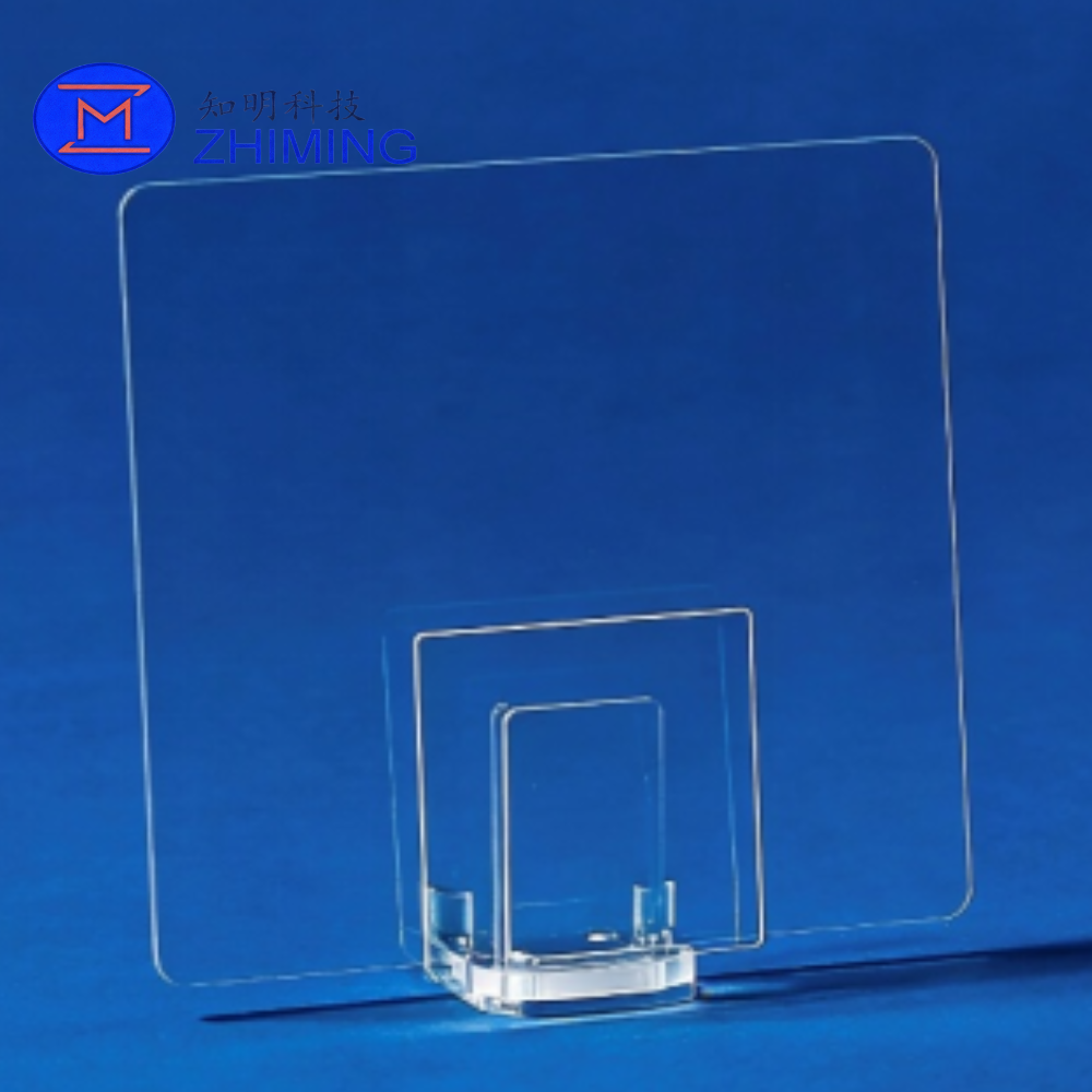
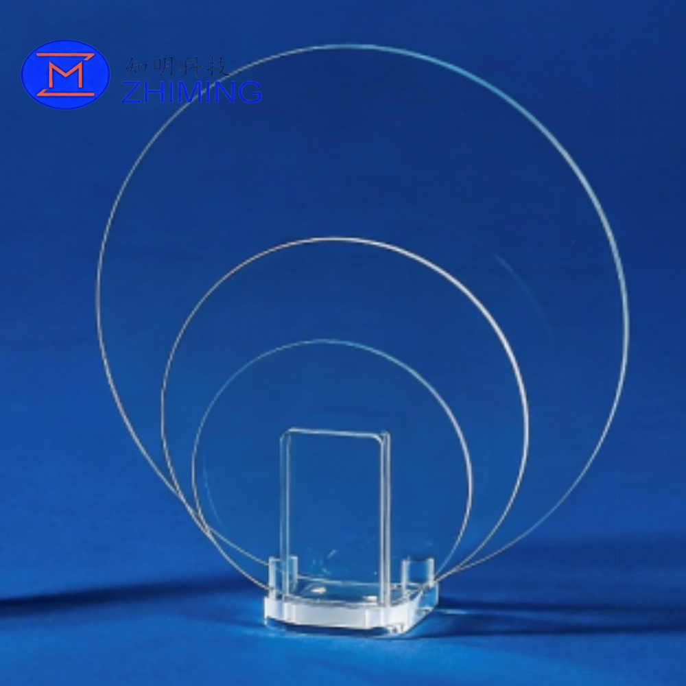
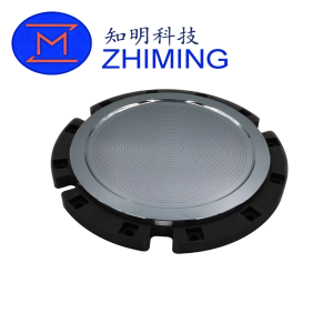
Tấm đế tạm thời bằng sapphire là một chất nền hiệu suất cao được thiết kế dành riêng cho các quy trình đóng gói bán dẫn tiên tiến, đặc biệt là trong các ứng dụng xử lý tấm wafer siêu mỏng và tích hợp dị chất.
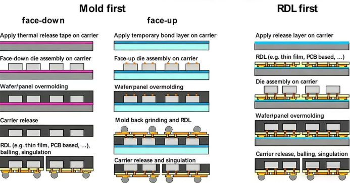
Công nghệ này được ứng dụng rộng rãi trong đóng gói IC 2.5D/3D, các quy trình TSV và RDL, đóng gói cấp tấm wafer/bảng mạch (FOWLP/FOPLP), cũng như các quy trình hàn tạm thời và tách rời.
Được thiết kế với độ cứng cực cao và tính ổn định nhiệt tuyệt vời, giá đỡ này cung cấp một nền tảng cơ học chính xác và ổn định cho quá trình mài mỏng và gia công mặt sau của tấm wafer, cho phép xử lý đáng tin cậy các tấm wafer có độ dày dưới 50 μm đồng thời duy trì tính toàn vẹn kích thước trong các điều kiện chu kỳ nhiệt phức tạp.
 Những thách thức trong ngành
Công nghệ đóng gói tiên tiến tiếp tục phát triển theo hướng cấu trúc mỏng hơn, kích thước lớn hơn và mật độ tích hợp cao hơn. Tuy nhiên, sự không ổn định trong quy trình sản xuất vẫn là một trở ngại quan trọng.
Các thách thức kỹ thuật chính bao gồm:
- Sự không tương thích về hệ số giãn nở nhiệt (CTE) giữa các vật liệu đóng gói khác nhau
- Sự tích tụ ứng suất trong các chu kỳ nhiệt lặp đi lặp lại
- Sự co ngót khi keo đông cứng và biến dạng tại giao diện
- Sự phân bố độ dày không đồng đều trong các chồng tấm wafer siêu mỏng
- Sự sai lệch định hướng do biến dạng và tổn thất năng suất
- Tính dễ vỡ cơ học của các tấm wafer siêu mỏng trong quá trình xử lý và chuyển giao
Những vấn đề này có tác động đáng kể đến hiệu suất sản xuất, độ tin cậy và khả năng mở rộng quy mô trong lĩnh vực sản xuất bao bì tiên tiến.
 Giải pháp: Nền tảng Sapphire Carrier
Sapphire là vật liệu lý tưởng để chế tạo các giá đỡ wafer tạm thời nhờ sự kết hợp tự nhiên giữa độ bền cơ học, độ trong suốt quang học và tính ổn định nhiệt.
Nó cho phép:
- Giá đỡ cơ khí có độ chính xác cao dành cho các tấm wafer siêu mỏng
- Giảm hiện tượng cong vênh và biến dạng trong quá trình gia công
- Khả năng tương thích với các công nghệ tách lớp bằng laser
- Phân bố ứng suất đồng đều trên các chất nền có diện tích lớn
- Hiệu suất ổn định trong điều kiện nhiệt độ cao và môi trường hóa chất
Những ưu điểm chính về hiệu suất
Mô đun Young cao (345–420 GPa)
Cung cấp độ cứng vượt trội, giúp hạn chế hiệu quả hiện tượng uốn cong của tấm wafer và biến dạng cấu trúc trong các quy trình nhiệt và cơ học.
Độ bền cơ học cao (1800–2200 HV)
Đảm bảo khả năng chống chịu cao trước các hư hỏng bề mặt và mài mòn cơ học, giúp sản phẩm có thể tái sử dụng lâu dài trong môi trường công nghiệp.
Độ truyền sáng cao (>83%, 300–1200 nm)
Giúp truyền dẫn tia laser hiệu quả, hỗ trợ các quy trình tách lớp bằng laser tiên tiến và các quy trình kết dính tạm thời.
Độ đồng đều vật liệu tuyệt vời
Giảm thiểu sự biến động của ứng suất cục bộ trên các tấm nền khổ lớn, từ đó nâng cao tính nhất quán của quy trình và sự ổn định của năng suất.
Độ ổn định nhiệt và hóa học vượt trội
Giữ được tính toàn vẹn cấu trúc trong điều kiện thay đổi nhiệt độ lặp đi lặp lại và làm sạch bằng hóa chất.
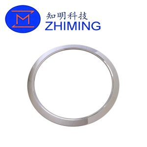
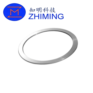
Thông số kỹ thuật
Hình học & Định dạng
| Tham số | Thông số kỹ thuật |
|---|---|
| Kích thước tấm wafer | 8 inch / 12 inch |
| Kích thước bảng điều khiển | 100 × 100 mm đến 510 × 515 mm |
| Phạm vi độ dày | 0,7 – 2,0 mm |
Hiệu suất về kích thước và bề mặt
| Bất động sản | Loại tiêu chuẩn | Loại có độ chính xác cao |
|---|---|---|
| Độ dao động tổng thể về độ dày (TTV) | ≤ 3 μm | ≤ 2 μm |
| Warp | ≤ 100 μm | ≤ 50 μm |
| Dung sai độ dày | ±0,010 mm | ±0,005 mm |
| Độ nhám bề mặt (Ra) | < 1,0 nm | < 1,0 nm |
| Xước/Cào | 60/40 | 40/20 |
Tính chất vật liệu
| Bất động sản | Giá trị |
|---|---|
| Hệ số đàn hồi của Young | 345 – 420 GPa |
| Độ cứng Vickers | 1.800 – 2.200 V |
| Hệ số truyền sáng | >83% (300–1200 nm) |
| Mật độ | 3,98 g/cm³ |
| Độ dẫn nhiệt | 30–40 W/m·K |
| CTE (20°C) | 5,6 – 7,7 × 10⁻⁶/K |
 Lĩnh vực ứng dụng
- Quy trình gia công mặt sau của tấm wafer siêu mỏng
- Tích hợp dị thể 2.5D / 3D
- Quy trình sản xuất TSV (Through-Silicon Via)
- Quá trình hình thành lớp phân phối lại (RDL)
- Hệ thống dán và tách wafer tạm thời
- Đóng gói cấp tấm bán dẫn phân tán (FOWLP)
- Bao bì cấp bảng mạch phân nhánh (FOPLP)
- Công nghệ mài mỏng và xử lý tấm wafer tiên tiến (tấm wafer dày dưới 50 μm)
Giá trị kỹ thuật
Khay đựng wafer tạm thời bằng sapphire giúp các nhà sản xuất bao bì tiên tiến đạt được:
- Giảm đáng kể hiện tượng cong vênh của tấm wafer và biến dạng cấu trúc
- Nâng cao độ chính xác trong việc căn chỉnh trong các quy trình đóng gói có khoảng cách chân linh kiện nhỏ
- Khả năng xử lý ổn định các tấm wafer siêu mỏng có độ dày dưới 50 μm
- Tăng cường tính ổn định về năng suất trong sản xuất quy mô lớn
- Nâng cao tính lặp lại của quy trình và sự ổn định trong sản xuất
- Khả năng tương thích với các nền tảng tích hợp đa nền tảng thế hệ mới
Câu hỏi thường gặp
Câu hỏi 1: Ưu điểm chính của sapphire trong các khay đựng wafer tạm thời là gì?
A: Sapphire mang lại độ cứng, độ bền và tính ổn định nhiệt cực cao, giúp kiểm soát hiện tượng cong vênh hiệu quả và đảm bảo độ tin cậy cơ học trong các quy trình đóng gói tiên tiến.
Câu hỏi 2: Sapphire có phù hợp cho các quy trình tách lớp bằng laser không?
A: Đúng vậy. Độ truyền sáng cao của vật liệu này trong dải bước sóng từ tia cực tím (UV) đến hồng ngoại trung (mid-IR) giúp tia laser xuyên qua hiệu quả, nhờ đó vật liệu này hoàn toàn tương thích với các hệ thống tách lớp bằng laser.
Câu hỏi 3: Các chất nền sapphire có thể hỗ trợ đóng gói tấm nền khổ lớn không?
A: Đúng vậy. Các tấm nền sapphire có thể được sản xuất với kích thước tấm lớn mà vẫn đảm bảo độ phẳng tuyệt vời và phân bố ứng suất đồng đều, nhờ đó rất phù hợp cho các ứng dụng đóng gói tiên tiến diện tích lớn như FOPLP và các ứng dụng khác.

Đánh giá
Chưa có đánh giá nào.