
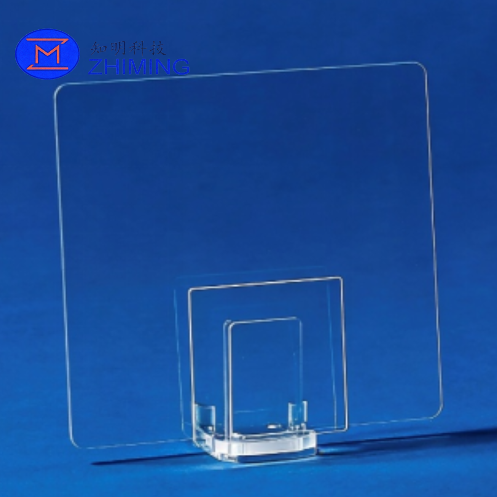
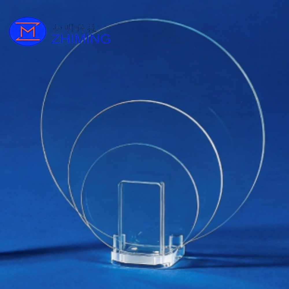
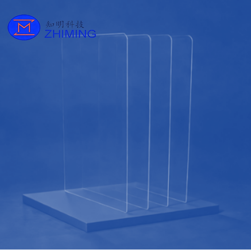
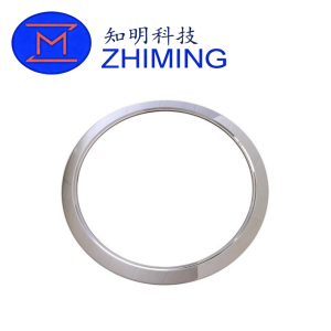
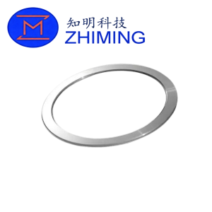
Dočasný nosič destiček ze safíru je vysoce výkonný substrát navržený pro pokročilé procesy balení polovodičů, zejména pro manipulaci s ultratenkými destičkami a aplikace v oblasti heterogenní integrace.
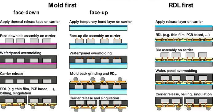
Široce se využívá při balení integrovaných obvodů 2,5D/3D, v procesech TSV a RDL, při balení typu fan-out na úrovni destiček a panelů (FOWLP/FOPLP) a v pracovních postupech dočasného spojování a odpojování.
Tento nosič, navržený s ohledem na mimořádnou tuhost a vynikající tepelnou stabilitu, poskytuje přesnou a stabilní mechanickou platformu pro ztenčování destiček a zpracování jejich zadní strany. Umožňuje tak spolehlivou manipulaci s destičkami o tloušťce nižší než 50 μm při zachování rozměrové stability i za náročných podmínek teplotních cyklů.
 Výzvy v odvětví
Pokročilé balení se neustále vyvíjí směrem k tenčím strukturám, větším formátům a vyšší hustotě integrace. Nestabilita výrobního procesu však zůstává zásadním úskalím.
Mezi hlavní technické výzvy patří:
- Nesoulad koeficientů tepelné roztažnosti (CTE) u různých obalových materiálů
- Hromadění napětí při opakovaných teplotních cyklech
- Smršťování lepidla při vytvrzování a deformace na rozhraní
- Nerovnoměrné rozložení tloušťky v souborech ultratenkých destiček
- Odchylka vyrovnání způsobená deformací a ztráta výtěžnosti
- Mechanická křehkost ultratenkých destiček při manipulaci a přenosu
Tyto problémy mají významný dopad na výtěžnost, spolehlivost a škálovatelnost procesů při výrobě moderních obalových systémů.
 Řešení: Platforma Sapphire Carrier
Safír představuje ideální materiálovou platformu pro dočasné nosiče destiček díky své přirozené kombinaci mechanické pevnosti, optické průhlednosti a tepelné stability.
Umožňuje:
- Vysoce přesná mechanická podpora pro ultratenké destičky
- Menší zkroucení a deformace během zpracování
- Kompatibilita s technologiemi odlepování využívajícími laser
- Rovnoměrné rozložení napětí na podkladech s velkou plochou
- Stabilní výkon v prostředí s vysokými teplotami a v chemickém prostředí
Hlavní výhody z hlediska výkonu
Vysoký modul pružnosti (345–420 GPa)
Zajišťuje mimořádnou tuhost a účinně potlačuje ohýbání destiček a deformaci konstrukce během tepelných a mechanických procesů.
Vysoká mechanická pevnost (1800–2200 HV)
Zajišťuje vysokou odolnost proti poškození povrchu a mechanickému opotřebení, což umožňuje dlouhodobé opakované použití v průmyslovém prostředí.
Vysoká optická propustnost (>83%, 300–1200 nm)
Umožňuje efektivní přenos laserového záření a podporuje pokročilé procesy odlepování laserem i dočasného lepení.
Vynikající rovnoměrnost materiálu
Minimalizuje lokální kolísání napětí na velkoformátových nosičích, čímž zvyšuje konzistenci procesu a stabilitu výtěžnosti.
Vynikající tepelná a chemická stabilita
Zachovává si strukturální integritu i při opakovaných teplotních cyklech a chemickém čištění.
Technické specifikace
Geometrie a formáty
| Parametr | Specifikace |
|---|---|
| Velikost oplatky | 8 palců / 12 palců |
| Velikost panelu | 100 × 100 mm až 510 × 515 mm |
| Rozsah tloušťky | 0,7 – 2,0 mm |
Rozměrové a povrchové vlastnosti
| Majetek | Standardní kvalita | Vysoce přesná třída |
|---|---|---|
| Celková odchylka tloušťky (TTV) | ≤ 3 μm | ≤ 2 μm |
| Warp | ≤ 100 μm | ≤ 50 μm |
| Tolerance tloušťky | ±0,010 mm | ±0,005 mm |
| Drsnost povrchu (Ra) | < 1,0 nm | < 1,0 nm |
| Škrábat/kopat | 60/40 | 40/20 |
Vlastnosti materiálu
| Majetek | Hodnota |
|---|---|
| Youngův modul | 345–420 GPa |
| Vickersova tvrdost | 1800–2200 HV |
| Optická propustnost | >83% (300–1200 nm) |
| Hustota | 3,98 g/cm³ |
| Tepelná vodivost | 30–40 W/m·K |
| CTE (20 °C) | 5,6 – 7,7 × 10⁻⁶/K |
 Oblasti použití
- Zpracování zadní strany ultratenkých destiček
- 2,5D / 3D heterogenní integrace
- Výroba TSV (průchozí křemíkové propojky)
- Vytvoření vrstvy RDL (Redistribution Layer)
- Systémy pro dočasné spojování a oddělování destiček
- Balení typu Fan-out na úrovni destičky (FOWLP)
- Balení na úrovni panelu s rozvětvením vývodů (FOPLP)
- Pokročilé ztenčování a manipulace s destičkami (destičky <50 μm)
Technická hodnota
Díky dočasnému nosiči z safíru mohou výrobci pokročilých obalových řešení dosáhnout:
- Výrazné snížení prohýbání destiček a strukturálních deformací
- Zvýšená přesnost vyrovnání při montáži součástek s malým roztečem
- Spolehlivá manipulace s ultratenkými destičkami o tloušťce pod 50 μm
- Vyšší konzistence výtěžnosti při výrobě ve velkém měřítku
- Zlepšená opakovatelnost procesu a stabilita výroby
- Kompatibilita s heterogenními integračními platformami nové generace
ČASTO KLADENÉ DOTAZY
Otázka 1: Jaká je hlavní výhoda použití safíru v dočasných nosičích destiček?
Odpověď: Safír se vyznačuje mimořádně vysokou tuhostí, tvrdostí a tepelnou stabilitou, což umožňuje vynikající kontrolu nad deformacemi a mechanickou spolehlivost v pokročilých procesech balení.
Otázka 2: Je safír vhodný pro procesy laserového odlepování?
Odpověď: Ano. Díky vysoké optické propustnosti v rozsahu vlnových délek od UV až po střední infračervené záření umožňuje účinné pronikání laserového paprsku, a je tak plně kompatibilní se systémy pro odlepování pomocí laseru.
Otázka 3: Jsou safírové nosiče vhodné pro balení velkoformátových panelů?
Odpověď: Ano. Safírové nosiče lze vyrábět ve velkých rozměrech při zachování vynikající rovinnosti a rovnoměrného rozložení napětí, díky čemuž jsou vhodné pro technologii FOPLP a další pokročilé aplikace v oblasti velkoplošného balení.
Recenze
Zatím zde nejsou žádné recenze.