

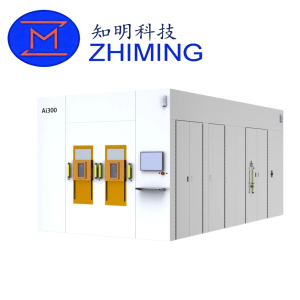
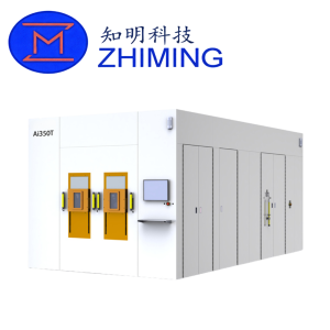
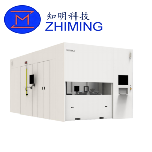
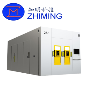
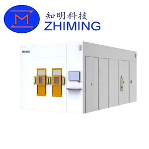
 The Ai300 (Medium Beam) high temperature ion implantation system is designed for 12-inch silicon wafer semiconductor manufacturing lines. It is a medium current ion implanter developed for advanced doping processes in both silicon-based and wide bandgap semiconductor applications, including SiC process lines.
The system supports an energy range from 5 keV to 300 keV, enabling flexible implantation from shallow junction formation to deep doping applications. It is equipped with a high temperature heated wafer stage with a maximum temperature up to 400°C, allowing improved dopant activation and reduced lattice damage during implantation.
With stable beam performance, high precision control, and compatibility with large-scale integrated circuit processes, the Ai300 system is suitable for advanced semiconductor manufacturing environments.
Features
High Temperature Implant Capability
Equipped with a heated wafer stage supporting temperatures up to 400°C, improving implantation quality and dopant activation efficiency.
Wide Energy Range
Energy range of 5–300 keV supports both shallow and deep implantation processes for advanced device structures.
High Precision Beam Control
Provides high accuracy implantation with angle accuracy ≤ 0.1°, beam parallelism ≤ 0.1°, uniformity ≤ 0.5%, and repeatability ≤ 0.5%.
High Throughput Performance
Supports throughput up to ≥ 500 wafers per hour, suitable for high-volume semiconductor manufacturing.
Advanced Ion Source Capability
Supports multiple implanted elements including C, B, P, N, He, and Ar, meeting diverse semiconductor process requirements.
LSI Process Compatibility
Fully compatible with large-scale integrated circuit manufacturing processes and advanced device fabrication.
Viktiga specifikationer
Process Parameters
| Föremål | Specifikation |
|---|---|
| Wafer-storlek | 12 inch |
| Energy Range | 5–300 keV |
| Implanted Elements | C, B, P, N, He, Ar |
| Dose Range | 1E11–1E16 ions/cm² |
Beam Performance
| Föremål | Specifikation |
|---|---|
| Beam Stability | ≤ 10% / hour (≤1 beam interruption or arcing per hour) |
| Beam Parallelism | ≤ 0.1° |
Implantation Accuracy
| Föremål | Specifikation |
|---|---|
| Implant Angle Range | 0°–45° |
| Angle Accuracy | ≤ 0.1° |
| Uniformity (1σ) | ≤ 0.5% (P+, 1E14, 100 keV) |
| Repeatability (1σ) | ≤ 0.5% |
System Performance
| Föremål | Specifikation |
|---|---|
| Genomströmning | ≥ 500 wafers per hour |
| Maximum Implant Temperature | 400°C |
| Equipment Size | 6400 × 3640 × 3100 mm |
| Vakuumnivå | 5E-7 Torr |
| X-ray Leakage | ≤ 0.3 μSv/h |
| Scanning Mode | Horizontal electrostatic scanning + vertical mechanical scanning |
Application Fields
SiC Semiconductor Processing
Used in silicon carbide device fabrication, supporting high temperature implantation processes required for wide bandgap materials.
Silicon-Based Semiconductor Manufacturing
Applicable to 12-inch silicon wafer production lines for CMOS and advanced integrated circuit fabrication.
High Temperature Implantation Processes
Supports implantation processes requiring elevated wafer temperature to reduce defects and improve dopant activation.
Power Device Fabrication
Suitable for power semiconductor devices where precise doping and high energy implantation are required.
Advanced Integrated Circuit Production
Supports LSI process integration with high precision and high throughput requirements.
Vanliga frågor och svar
1. What wafer size does the Ai300 system support
The system is designed for 12-inch silicon wafers and is suitable for advanced semiconductor manufacturing lines.
2. What is the key advantage of the high temperature implantation capability
The system supports implantation up to 400°C, which helps reduce lattice damage, improve dopant activation, and enhance overall device performance.
3. What level of precision and production efficiency does the system provide
The system provides angle accuracy within 0.1 degrees, beam parallelism within 0.1 degrees, and uniformity and repeatability within 0.5 percent, with throughput up to 500 wafers per hour.
Recensioner
Det finns inga recensioner än.