
Artificial intelligence is changing the physical architecture of semiconductor packages.
For many years, semiconductor performance improvements were driven primarily by transistor scaling. Today, leading AI accelerators increasingly depend on another type of scaling:
bringing more logic, memory and chiplets together inside one package.
This is why advanced packaging technologies such as TSMC’s CoWoS have become strategically important.
At the center of many of these packages is a component that receives far less attention than the GPU or HBM mounted on top of it:
the silicon interposer.
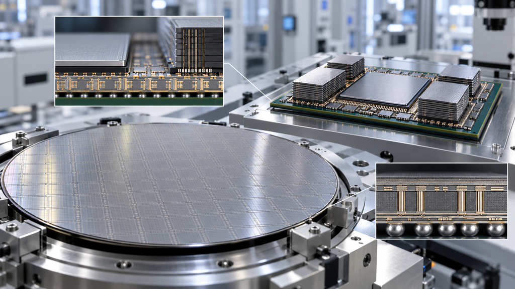
A silicon interposer provides the high-density electrical connections that allow processors, chiplets and High Bandwidth Memory to communicate over very short distances.
As AI packages become larger and incorporate more HBM stacks, the interposer must also scale.
That means the industry’s challenge is no longer simply producing silicon interposers.
It is producing:
larger, thinner, flatter and more tightly controlled silicon interposers at high yield.
This trend became especially visible on October 8, 2026, when GlobalFoundries announced a manufacturing agreement with TSMC to establish a U.S.-based supply of silicon interposers for TSMC’s CoWoS advanced packaging ecosystem.
The new capacity at GlobalFoundries’ Malta, New York facility will support growing AI and high-performance-computing demand.
This is an important signal.
Silicon interposers are becoming a critical part of the AI semiconductor supply chain.
What Is a Silicon Interposer?
A silicon interposer is a thin piece of silicon positioned between semiconductor dies and the package substrate.
Unlike a conventional silicon device wafer, the interposer does not necessarily contain large numbers of active transistors.
Its primary purpose is to provide extremely dense electrical routing.
A simplified AI package may look like:
GPU / AI Accelerator + HBM → Silicon Interposer → Package Substrate → PCB
The interposer provides short, high-density electrical connections between the components mounted above it.
It may contain:
- fine-pitch copper redistribution layers;
- Through-Silicon Vias;
- microbumps;
- power distribution structures;
- embedded passive structures;
- and high-density signal routing.
This architecture allows an AI processor and several HBM stacks to communicate at extremely high bandwidth.
TSMC describes silicon interposers as one of the key technologies for high-density chip-to-chip interconnection in HPC and AI applications.
Why AI Needs Silicon Interposers
AI processors need enormous amounts of data.
A processor may contain tremendous computing capability, but that capability becomes less useful if data cannot move between memory and logic fast enough.
Traditional off-package memory connections require signals to travel longer distances through the package substrate and printed circuit board.
HBM changes this architecture.
Multiple DRAM dies are vertically stacked, and those HBM stacks are placed close to the processor.
The silicon interposer then creates dense, short connections between:
Logic ↔ HBM
This reduces interconnect distance and enables extremely high memory bandwidth.
Applied Materials describes advanced packaging as a critical enabler of AI scaling because bringing compute and memory physically closer together improves data-transfer speed and energy efficiency.
The result is a major shift in semiconductor design.
Instead of asking only:
How many transistors can fit inside one chip?
engineers are increasingly asking:
How many high-performance dies can be efficiently integrated inside one package?
That is precisely where silicon interposers become important.
CoWoS-S: The Silicon Interposer Architecture
TSMC’s CoWoS platform includes several architectures.
The three major versions are:
- CoWoS-S;
- CoWoS-L;
- CoWoS-R.
They should not be treated as identical.
CoWoS-S
CoWoS-S uses a silicon interposer.
The interposer can contain high-density routing, TSVs and integrated capacitor structures.
Logic dies and HBM stacks are placed on top.
TSMC currently states that CoWoS-S can accommodate silicon interposers up to approximately 3.3× reticle size, or around 2,700 mm².
CoWoS-R
CoWoS-R uses an RDL interposer based primarily on polymer and copper redistribution structures rather than a full large silicon interposer.
CoWoS-L
CoWoS-L combines large RDL-based structures with localized silicon interconnects.
This allows package dimensions to continue increasing without requiring the complete interposer area to be monolithic silicon.
TSMC’s first 3.5×-reticle CoWoS-L entered volume production in 2024, and larger architectures are continuing to develop for AI applications.
These alternatives show an important industry reality:
silicon provides exceptional interconnect density, but scaling a very large silicon interposer becomes progressively more difficult and expensive.
Silicon Interposers Are Becoming Much Larger
One of the clearest trends in CoWoS development is increasing interposer area.
Earlier generations were close to one reticle in size.
Over time, the industry moved toward:
approximately 1× reticle
→ 2× reticle
→ 3× reticle
→ 3.3× reticle and beyond.
TSMC previously demonstrated a roughly 2,500 mm² three-reticle silicon interposer capable of accommodating multiple logic chips together with eight HBM stacks.
Today, TSMC lists CoWoS-S silicon interposer capability at approximately 2,700 mm².
Why does the area continue increasing?
Because AI systems want to integrate:
- larger compute dies;
- more chiplets;
- more HBM stacks;
- more memory capacity;
- more I/O;
- and more power-delivery structures.
A larger interposer creates more space for integration.
But larger area also creates new manufacturing problems.
Why Large-Area Silicon Interposers Are Difficult
A silicon interposer cannot simply be enlarged without consequences.
As area increases, manufacturers must control:
- wafer thickness;
- TTV;
- Bow;
- Warp;
- TSV uniformity;
- RDL uniformity;
- copper density;
- residual stress;
- thermal expansion;
- bump coplanarity;
- and mechanical handling.
Even relatively small dimensional deviations can create significant problems over a very large package.
This is why low-warp interposer manufacturing is increasingly important.
1. Bow and Warp Become More Critical as Area Increases
A perfectly flat interposer is the ideal condition.
In reality, semiconductor structures contain multiple materials with different mechanical and thermal properties.
These may include:
silicon, copper, dielectric films, polymers, underfill and organic substrate materials.
When the temperature changes, these materials expand by different amounts.
This creates stress.
That stress can deform the interposer or complete package.
Warpage is already recognized as a major problem in advanced packaging because larger heterogeneous packages combine materials with different coefficients of thermal expansion.
The problem becomes more serious as package dimensions increase.
A small curvature over a short distance may be manageable.
The same curvature across a much larger interposer can create significant height variation between opposite regions of the package.
Why Warpage Matters
Excessive warpage can affect multiple manufacturing steps.
Die Placement
Logic and HBM dies must be placed accurately.
If the interposer surface is not sufficiently planar, the bonding gap may vary from one area to another.
Microbump Bonding
Large AI packages can contain huge numbers of interconnects.
Poor coplanarity increases the risk of incomplete electrical connections.
Lithography
Interposer redistribution layers require precise patterning.
Excessive Bow or Warp can affect focus and alignment.
Temporary Bonding
Thin interposers may require carrier support during processing.
Geometry changes can complicate carrier bonding and debonding.
Package Assembly
The final interposer must eventually connect to an organic package substrate.
Warpage at this stage can create solder-joint reliability problems.
TSMC encountered warpage challenges even in earlier generations of large-area CoWoS. Its published work on a 1,200 mm² interposer noted that package yield required solving warpage associated with the large heterogeneous structure.
Today’s AI packages are considerably larger.
That makes the problem even more important.
2. TTV Becomes a Key Starting Material Parameter
Before complex RDL, TSV and packaging structures are added, the silicon substrate itself must already have tightly controlled geometry.
One important parameter is:
Total Thickness Variation — TTV
TTV is the difference between the maximum and minimum thickness across a wafer or interposer.
Low TTV becomes important during:
- wafer thinning;
- lithography;
- temporary bonding;
- CMP;
- TSV reveal;
- backside processing;
- and bonding.
For example, if a silicon interposer needs to be thinned before TSV exposure, an initial thickness variation can translate into non-uniform backside processing.
Therefore, specifying only:
“silicon wafer thickness = X µm”
is not enough.
The manufacturer also needs to consider:
How uniform is that thickness across the entire usable area?
3. TSVs Make Silicon Interposers Different from Simple Silicon Plates
A silicon interposer is not simply a polished silicon wafer.
One of its defining technologies is the Through-Silicon Via.
TSVs create vertical electrical paths through the silicon.
A simplified process can include:
- TSV lithography;
- silicon etching;
- dielectric liner deposition;
- barrier and seed formation;
- copper electroplating;
- CMP;
- wafer thinning;
- backside TSV reveal;
- redistribution-layer processing.
Each step introduces additional process variation.
Important TSV parameters include:
- via diameter;
- via depth;
- aspect ratio;
- sidewall profile;
- copper fill;
- void formation;
- resistance;
- pitch;
- and positional accuracy.
As interposer area increases, manufacturers must maintain TSV consistency across a much larger processing surface.
4. Copper Creates Both Electrical Benefits and Mechanical Challenges
Copper is essential to advanced packaging.
It provides low-resistance electrical routing and vertical interconnection.
However, copper and silicon have significantly different thermal expansion behavior.
This matters because an interposer may contain a very large amount of copper distributed through:
- TSVs;
- RDL;
- microbumps;
- power-delivery structures.
Non-uniform copper density can generate local stress.
This can affect:
- wafer curvature;
- local surface deformation;
- CMP behavior;
- and bonding coplanarity.
This is why advanced packaging warpage should not be understood only as a simple global Bow measurement.
Local surface shape is also increasingly important.
Recent industry discussion around AI packaging emphasizes that local slope, die-to-die coplanarity, bonding deformation, CMP and CTE mismatch can all affect yield as packages become larger.
5. Interposer Thickness Is a Trade-Off
A thicker silicon interposer offers greater mechanical rigidity.
But it also creates challenges.
Longer TSVs generally require:
- deeper etching;
- higher aspect ratios;
- more copper filling;
- and greater processing complexity.
A thinner interposer shortens the vertical electrical path and may simplify some TSV requirements.
However, thin silicon becomes mechanically fragile.
It becomes more susceptible to:
- Bow;
- Warp;
- breakage;
- edge damage;
- and handling problems.
This means interposer thickness cannot be optimized independently.
It must be selected together with:
TSV architecture + mechanical stability + temporary carrier process + package design.
6. HBM Is Increasing the Mechanical Challenge
The interposer itself is only one part of the package.
HBM introduces another important mechanical factor.
HBM consists of multiple vertically stacked DRAM dies.
As memory capacity increases, stack height and layer count also increase.
At the same time, individual memory dies must become extremely thin.
Applied Materials stated in 2026 that advanced HBM dies may be thinned to roughly 1/25 the thickness of a conventional DRAM wafer, making them highly susceptible to deformation and warpage.
As HBM moves toward 12-, 16-layer and future higher stacks, controlling mechanical stress becomes increasingly important.
Now combine:
large silicon interposer + large logic die + multiple HBM stacks + organic substrate
and the mechanical challenge becomes clear.
Low warpage must be managed across the complete package, not only one individual material.
7. Interposer Size Is Also a Lithography Problem
Conventional semiconductor lithography is limited by the exposure field of the reticle.
Modern AI interposers can be much larger than one reticle.
The solution is reticle stitching.
Instead of exposing the entire interposer pattern at once, multiple exposure fields are stitched together.
TSMC has used this strategy to progressively scale CoWoS silicon interposers beyond one reticle.
But stitching introduces additional requirements.
Patterns from neighboring exposure regions must align accurately.
This increases the importance of:
- wafer dimensional stability;
- lithography overlay;
- stage accuracy;
- surface flatness;
- film uniformity;
- and distortion control.
As interposers become larger, process uniformity becomes increasingly difficult.
8. Why Low Warp and High Flatness Are Different
These terms are sometimes used interchangeably, but they describe different aspects of wafer geometry.
Bow
Bow generally describes the displacement of the wafer’s median surface relative to a reference plane.
Warp
Warp describes the overall difference between the highest and lowest points of the median surface.
TTV
TTV describes thickness variation.
Local Flatness
Local flatness evaluates smaller regions rather than the entire interposer.
This distinction matters.
A wafer may have acceptable global Bow while still containing local surface distortion that affects bonding.
For fine-pitch advanced packaging, engineers increasingly need both:
global geometry control + local surface control.
9. Large Interposers Also Increase Defect Cost
Advanced AI packages are expensive.
A large interposer may support:
- one or more advanced logic dies;
- multiple HBM stacks;
- thousands of fine interconnects;
- and complex package processing.
A defect introduced late in the assembly process can therefore destroy a very high-value package.
Examples include:
- TSV voids;
- broken RDL traces;
- particles;
- bump-height variation;
- poor bonding;
- delamination;
- interposer cracking;
- and excessive warpage.
This is one reason advanced packaging is increasingly adopting inspection and metrology technologies previously associated with front-end semiconductor fabrication.
Applied Materials noted in June 2026 that advanced packaging structures now require wafer-fab-level process control because feature sizes are shrinking and defects can cause entire HBM stacks to be scrapped.
10. Why the GlobalFoundries–TSMC Agreement Matters
The October 2026 GlobalFoundries announcement is important beyond the individual companies involved.
GlobalFoundries will establish U.S.-based silicon interposer manufacturing capacity at its Malta, New York facility for TSMC’s CoWoS ecosystem.
This shows that silicon interposers are becoming strategically important enough to justify dedicated geographic supply-chain expansion.
The demand driver is straightforward:
AI accelerators need more advanced packaging.
More advanced packaging means more demand for:
- interposer processing;
- TSV fabrication;
- wafer thinning;
- RDL;
- advanced bonding;
- HBM integration;
- packaging substrates;
- and associated semiconductor materials.
According to reporting on the agreement, volume production is expected to begin ramping in the first half of 2028.
This should therefore be viewed not merely as another foundry agreement.
It is evidence that advanced packaging infrastructure is becoming a strategic part of semiconductor manufacturing capacity.
11. What Should Engineers Specify for Silicon Interposer Substrates?
When requesting silicon material for interposer development, simply specifying:
“300 mm silicon wafer”
is usually insufficient.
A useful specification should consider the intended downstream process.
Basic Dimensions
- diameter;
- thickness;
- thickness tolerance;
- notch specification;
- edge profile.
Wafer Geometry
- TTV;
- Bow;
- Warp;
- local flatness.
Surface Condition
- single-side or double-side polished;
- surface roughness;
- scratches;
- particles;
- surface defects.
Crystal and Electrical Properties
Depending on process requirements:
- crystal orientation;
- conductivity type;
- resistivity;
- doping;
- oxygen concentration.
Processing Requirements
If further processing is involved:
- TSV depth;
- target final thickness;
- temporary bonding requirement;
- backside grinding;
- CMP;
- RDL processing;
- dicing or singulation requirements.
The substrate specification should ultimately be linked to the complete interposer process flow.
12. From Silicon Wafer to Finished Interposer
A simplified silicon interposer manufacturing sequence may look like:
Silicon Wafer
↓
TSV Formation
↓
Dielectric / Barrier / Seed Layers
↓
Copper Filling
↓
CMP
↓
Front-Side RDL
↓
Temporary Bonding
↓
Backside Grinding / Thinning
↓
TSV Reveal
↓
Backside Metallization / Bumps
↓
Inspection
↓
Dicing
↓
Logic + HBM Integration
Every one of these processes can influence final geometry.
For example:
CMP can affect local flatness.
Thin-wafer grinding can influence Bow.
Copper deposition introduces stress.
Temporary bonding can alter wafer shape.
Dicing can generate edge damage.
For this reason, low-warp interposer production requires control of the entire manufacturing chain rather than simply starting with a flat silicon wafer.
Silicon Interposer vs RDL Interposer
As package dimensions continue increasing, one important question is:
Will silicon interposers continue scaling indefinitely?
Probably not in every application.
This is one reason CoWoS now includes multiple architectures.
Silicon Interposer
Advantages include:
- very fine routing;
- mature silicon processing;
- high interconnect density;
- TSV integration;
- high dimensional precision.
Challenges include:
- cost;
- large-area lithography;
- silicon area consumption;
- handling;
- warpage;
- reticle stitching.
RDL-Based Interposer
Potential advantages include:
- easier scaling to larger package dimensions;
- reduced dependence on large monolithic silicon;
- greater mechanical flexibility;
- potentially different cost structure.
TSMC itself recommends CoWoS-L or CoWoS-R for interposer dimensions beyond the current approximately 3.3×-reticle CoWoS-S range.
The future is therefore unlikely to be:
silicon interposer versus RDL interposer.
Instead, different architectures will coexist according to required:
density, package size, performance and cost.
The AI Packaging Race Is Becoming an Interposer Race
AI has made the semiconductor package part of system performance.
The processor can no longer be optimized separately from memory and interconnect.
The silicon interposer sits directly in the middle of this transformation.
It enables:
GPU ↔ HBM
Chiplet ↔ Chiplet
Logic ↔ Memory
through very dense, short electrical paths.
But every increase in AI package size creates a corresponding increase in manufacturing difficulty.
The next generation of silicon interposers must therefore deliver more than simply larger area.
They must combine:
large area + low TTV + low Bow and Warp + high TSV yield + fine RDL + precise bonding + strong mechanical reliability.
TSMC’s CoWoS roadmap already demonstrates this trend, with CoWoS-S silicon interposer dimensions having expanded significantly over successive generations and alternative CoWoS-L and CoWoS-R architectures being developed for still larger systems.
And the October 2026 GlobalFoundries–TSMC manufacturing agreement shows that silicon interposer capacity itself is now becoming part of the strategic AI semiconductor supply chain.
For semiconductor material suppliers, wafer manufacturers and precision processing companies, this creates a new set of opportunities.
The key question will no longer be simply:
Can we supply silicon?
It will be:
Can we supply and process silicon with the geometry, surface quality and consistency required for increasingly large AI interposers?
That distinction will become increasingly important as AI packaging moves toward larger, denser and more complex heterogeneous systems.