


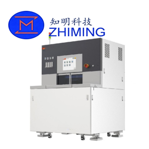
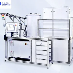
The 6/8/12-Inch LPCVD Oxidation Furnace is a state-of-the-art semiconductor manufacturing tool designed for precise and uniform thin-film deposition. It is widely applied in growing high-quality polysilicon, silicon nitride, and silicon oxide layers on wafers, ensuring consistent performance for power semiconductors, advanced substrates, and other high-precision applications.
This equipment combines advanced low-pressure deposition technology, intelligent temperature control, and ultra-clean process design to achieve exceptional thin-film uniformity and high throughput. Its vertical reactor configuration allows efficient batch processing, while its thermal deposition process avoids plasma-induced damage, making it ideal for critical processes such as gate dielectric formation, stress-buffering layers, and protective oxides.
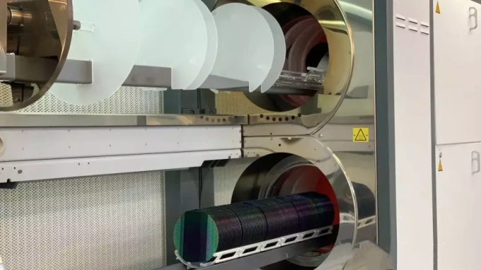
Key Advantages
- High Uniformity Thin-Film Deposition: Low-pressure environment (0.1–10 Torr) ensures wafer-to-wafer and within-wafer uniformity of ±1.5%, critical for high-performance device fabrication.
- Vertical Reactor Design: Handles 150–200 wafers per batch, improving throughput and production efficiency for industrial-scale semiconductor fabrication.
- Thermal Deposition Process (500–900°C): Provides gentle, plasma-free deposition to protect sensitive substrates and maintain high film quality.
- Intelligent Temperature Control: Real-time monitoring and adjustment with ±1°C accuracy for stable, repeatable results.
- Ultra-Clean Process Chamber: Minimizes particle contamination, supporting SiC and other advanced wafer materials.
- Customizable Configuration: Flexible design accommodates various process requirements, including dry or wet oxidation and different wafer sizes.
Technical Specifications
| Feature | Specification |
|---|---|
| Wafer Size | 6/8/12 Inch |
| Compatible Materials | Polysilicon, Silicon Nitride, Silicon Oxide |
| Oxidation Type | Dry Oxygen / Wet Oxygen (DCE, HCL) |
| Process Temperature Range | 500°C–900°C |
| Constant Temperature Zone | ≥800 mm |
| Temperature Control Accuracy | ±1°C |
| Particle Control | <15 EA (>0.32μm), <60 EA (>0.32μm), <80 EA (>0.226μm) |
| Film Thickness | NIT1500 ±50 Å |
| Uniformity | Within wafer <2.5%, wafer-to-wafer <2.5%, batch-to-batch <2% |
Product Features
- Automated wafer handling ensures high safety and operational efficiency.
- Ultra-clean process chamber reduces contamination risk and maintains consistent film quality.
- Superior film thickness uniformity supports advanced node manufacturing.
- Real-time intelligent temperature and pressure control allows precise process adjustments.
- SiC wafer support reduces friction and particle generation, extending wafer lifetime.
- Modular design enables customization for diverse applications and process needs.
Deposition Process Principle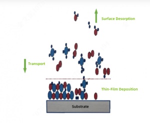
- Gas Introduction: Reactant gases are introduced into the tube under low-pressure conditions (0.25–1 Torr).
- Surface Diffusion: Molecules freely diffuse across the wafer surface, ensuring uniform coverage.
- Adsorption: Reactants adhere to the wafer surface before chemical reaction.
- Chemical Reaction: Thermal decomposition forms the desired thin film directly on the substrate.
- Byproduct Removal: Non-reactive gases are evacuated to maintain purity and prevent interference.
- Film Formation: Reaction products gradually accumulate, forming a uniform, stable thin-film layer.
Applications
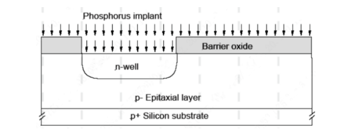
- Shielding Oxide Layer: Protects silicon wafers from contamination and reduces ion channeling during doping processes.
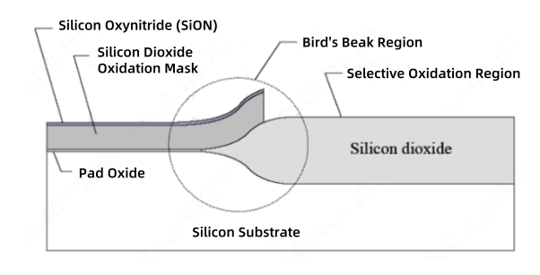
- Pad Oxide Layer: Acts as a stress buffer between silicon and silicon nitride layers, preventing wafer cracking and improving yield.
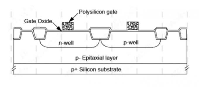
- Gate Oxide Layer: Provides the dielectric layer in MOS structures, ensuring precise current conduction and field-effect control.
System Configurations
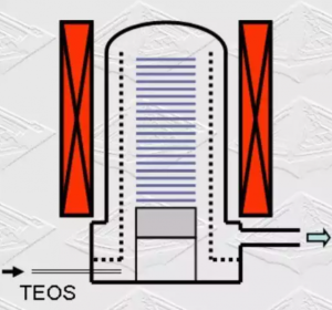
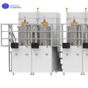
- Vertical LPCVD: Process gases flow from top to bottom, achieving uniform deposition on all wafers in a batch.
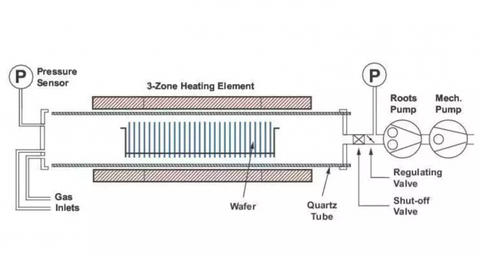
- Horizontal LPCVD: Gases flow along the length of the substrates, suitable for continuous, high-volume production, though deposition thickness may vary slightly near the inlet side.
Frequently Asked Questions
Q1: What is LPCVD primarily used for?
A: LPCVD is a low-pressure thin-film deposition process widely used in semiconductor manufacturing for polysilicon, silicon nitride, and silicon oxide deposition, enabling uniform and high-quality films for advanced device fabrication.
Q2: How does LPCVD differ from PECVD?
A: LPCVD relies on thermal activation under low pressure to produce high-purity films, while PECVD uses plasma at lower temperatures for faster deposition, often with slightly lower film quality.
Q3: What wafer sizes and materials are compatible with this LPCVD Oxidation Furnace?
A: This furnace supports 6-inch, 8-inch, and 12-inch wafers and is compatible with polysilicon, silicon nitride, silicon oxide, and SiC wafers, providing flexibility for various semiconductor applications.
Q4: Can the LPCVD Oxidation Furnace be customized for specific processes?
A: Yes, the system offers modular configurations, including adjustable temperature zones, gas flow control, and oxidation modes (dry or wet), allowing it to meet diverse process requirements for both research and industrial-scale production.
Request a Quote for 6/8/12-Inch LPCVD Oxidation Furnace High-Uniformity Thin-Film Deposition for Advanced Semiconductor Manufacturing
Tell us your required specifications, dimensions, quantity, application and technical requirements. You can also provide drawings or additional project information. Our technical team will review your requirements and reply as soon as possible.
Reviews
There are no reviews yet.