
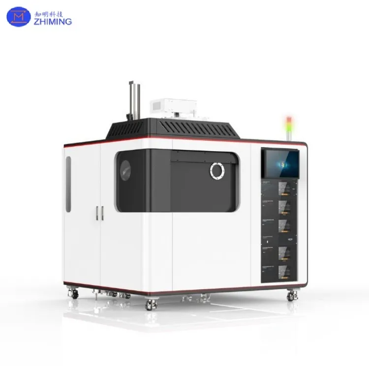
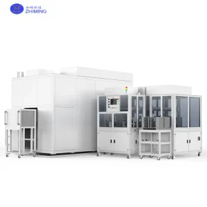
 The Ion Beam Etching Machine for Si, SiO2, and Metal Materials is a high-precision dry etching system designed for advanced microfabrication and nanotechnology applications. Utilizing ion beam etching (IBE), also known as ion milling, this equipment enables highly material removal through a purely physical sputtering process.
Unlike conventional plasma-based etching technologies, ion beam etching does not expose the substrate directly to plasma. This significantly reduces risks of plasma-induced damage, contamination, and charge accumulation, making it especially suitable for sensitive semiconductor and optical device manufacturing.
With nanometer-level precision and excellent process controllability, this system is widely used in semiconductor fabrication, thin film processing, and advanced materials research.
 Key Technical Features
- Ultra-High Precision
Achieves etching resolution of ≤10 nm, meeting advanced semiconductor and nanofabrication requirements. - Non-Selective Etching Capability
Enables uniform etching across multiple materials including metals, semiconductors, and dielectrics without chemical dependency. - Anisotropic and Directional Control
Adjustable ion beam angles allow both anisotropic and isotropic etching profiles, supporting complex pattern transfer. - Plasma-Free Processing Environment
Eliminates plasma-induced damage, ensuring higher device reliability and yield. - Excellent Surface Quality
Produces smooth surfaces with reduced roughness, critical for optical and electronic applications.
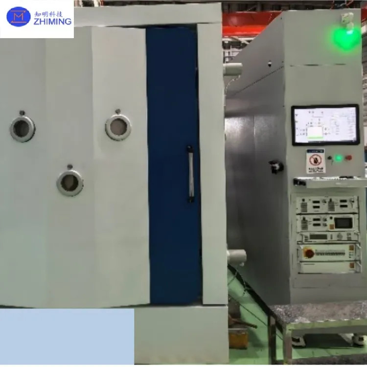
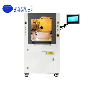
Core System Components
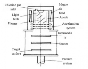
A complete ion beam etching system consists of several critical subsystems:
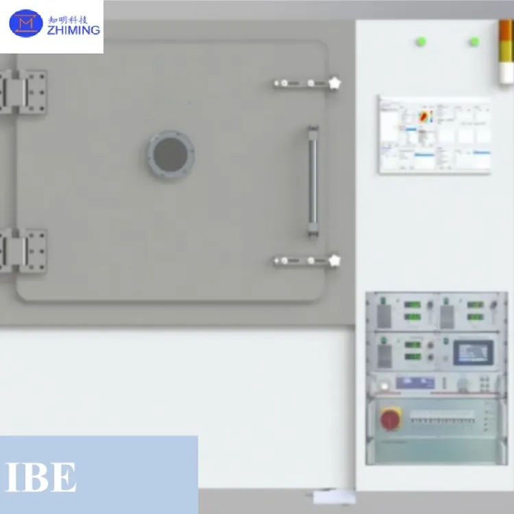
1. Vacuum System
Provides a high-vacuum environment essential for:
- Beam stability
- Contamination control
- High-precision processing
2. Ion Source
Generates a high-energy ion beam (commonly argon ions):
- Determines etching rate and uniformity
- Supports different source types such as RF and Kaufman ion sources
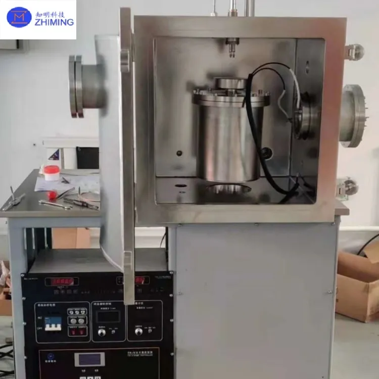
3. Sample Stage
- Supports multi-axis rotation for uniform etching
- Integrated temperature control improves process stability
4. Control System
- Fully automated operation
- Enables precise parameter control and repeatability
- Optional end-point detection for advanced process control
5. Neutralizer
- Prevents charge buildup during etching
- Essential for insulating materials such as SiO₂ and Si₃N₄
Working Principle
 Ion beam etching operates by directing a high-energy, collimated ion beam toward the target material surface under vacuum conditions.
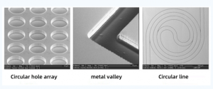
The ions (typically Ar⁺) collide with surface atoms, transferring momentum and causing atoms to be ejected via physical sputtering. This process removes material layer by layer, enabling precise pattern definition without chemical reactions.
This makes IBE particularly suitable for:
- High-resolution pattern transfer
- Materials with low chemical reactivity
- Multi-layer structures
Processing Capabilities
Supported Materials
- Metals: Au, Pt, Cu, Ta, Al
- Semiconductors: Si, GaAs
- Dielectrics: SiO₂, Si₃N₄
- Advanced Materials: AlN, ceramics, polymers
Typical Process Flow
- Sample Preparation
Clean and mount the substrate in the vacuum chamber - Masking
Apply photoresist or metal mask to define etching areas - Ion Beam Generation
Activate ion source using inert gas (typically argon) - Etching Process
Adjust beam energy, angle, and time to achieve desired structure - Mask Removal
Remove mask to reveal final etched patterns
Application Areas
 Semiconductor Manufacturing
- Integrated circuit patterning
- Thin film structuring
- Advanced node fabrication
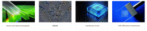
Optical Devices
- Precision processing of gratings and lenses
- Surface modification of optical components
Nanotechnology
- Fabrication of nanowires, nanopores, and MEMS structures
Materials Science
- Surface analysis and modification
- Functional coating preparation
Advantages Over Conventional Etching
| Feature | Ion Beam Etching | Reactive Ion Etching |
|---|---|---|
| Process Type | Physical | Physical + Chemical |
| Plasma Exposure | No direct exposure | Direct exposure |
| Material Selectivity | Low (uniform) | High |
| Surface Damage | Minimal | Possible |
| Precision | Ultra-high | High |
FAQ
What is ion beam etching?
Ion beam etching is a dry etching process that removes material through physical sputtering using high-energy ions in a vacuum environment.
IBE vs RIE difference?
- IBE: purely physical, no plasma contact, higher precision
- RIE: combines chemical reactions with plasma, higher selectivity but more risk of damage

Reviews
There are no reviews yet.