
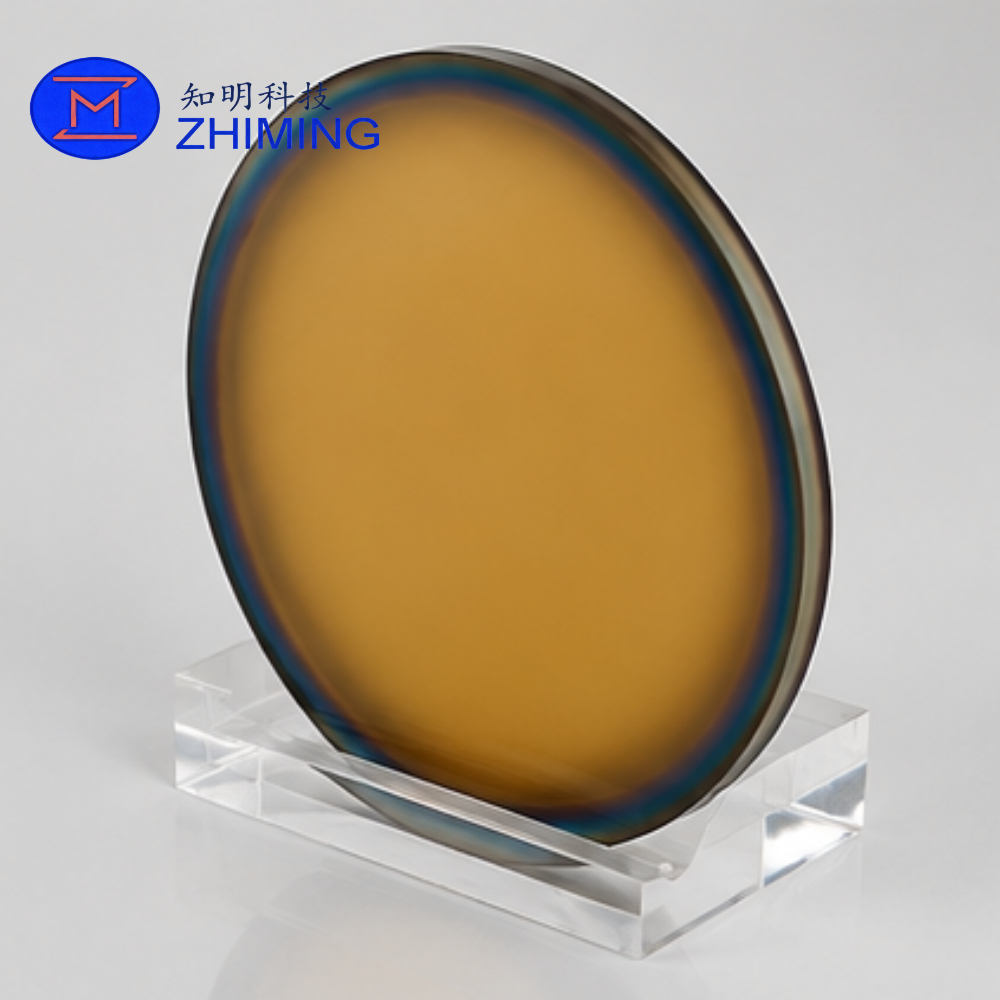


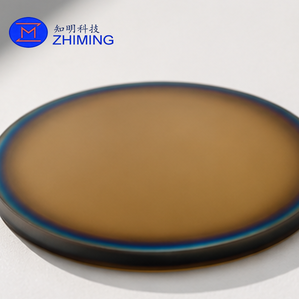
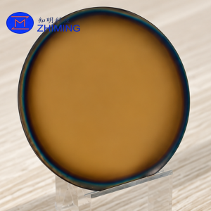
 Ultra-Thin Silicon-Integrated Diamond Film is a wafer-level thermal management material developed for advanced semiconductor devices requiring extreme heat dissipation performance. It is fabricated by directly depositing polycrystalline diamond onto silicon wafers using Microwave Plasma Chemical Vapor Deposition (MPCVD) technology.
With a controlled diamond layer thickness below 1 μm, this material enables near-junction thermal spreading, effectively reducing hotspot concentration and improving overall device thermal stability.
Unlike conventional thermal interface materials that are applied at the package level, this diamond film is integrated directly onto the silicon wafer, allowing heat to be managed at the source before it propagates through the device structure.
This makes it highly suitable for RF devices, power electronics, silicon photonics, and advanced semiconductor packaging architectures.
Belangrijkste voordelen
Near-Junction Heat Spreading
Direct integration on silicon wafers allows heat to be dissipated at the device level, significantly reducing thermal bottlenecks.
Ultra-Thin Diamond Layer (<1 μm)
Precise thickness control enables high thermal performance without adding mechanical stress or excessive material volume.
Direct Wafer Integration
Eliminates additional thermal interface layers, reducing thermal resistance and improving system efficiency.
High Thermal Conductivity Material
Diamond provides one of the highest known thermal conductivities, enabling rapid lateral heat spreading across the wafer surface.
Semiconductor Process Compatible
Fully compatible with standard silicon wafer fabrication processes, supporting scalable industrial production.
Multi-Wafer Size Availability
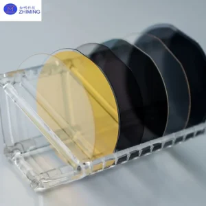
Supports 4-inch, 6-inch, and 8-inch silicon wafers for different device and manufacturing requirements.
Technische specificaties
| Parameter | Specificatie |
|---|---|
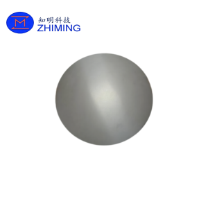
| Material System | Polycrystalline Diamond on Silicon |
| Growth Technology | MPCVD (Microwave Plasma CVD) |
| Substraat | Siliciumwafel |
| Wafer Sizes | 4″, 6″, 8″ |
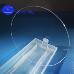
| Diamond Thickness | < 1 μm (Ultra-Thin Control) |
| Thermische geleidbaarheid | Ultra-High (Diamond-Based) |
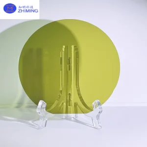
| Oppervlaktegesteldheid | As-grown / Polished Options |
| Integration Level | Wafer-Level Integration |
| Maatwerk | Thickness, wafer size, process tuning available |
Performance Benefits Compared to Conventional Thermal Solutions
| Eigendom | Silicon-Integrated Diamond Film | Traditional Thermal Materials |
|---|---|---|
| Heat Spreading Location | Wafer-Level (Near Junction) | Package-Level |
| Thermische geleidbaarheid | Extremely High | Medium |
| Thermal Resistance | Zeer laag | Hoger |
| Dikte | <1 μm | Tens–Hundreds μm |
| Integration Complexity | Low (In-process) | Additional Assembly Required |
| Hotspot Control | Uitstekend | Beperkt |
Toepassingsgebieden
RF & Microwave Devices
Ideal for GaN HEMTs, RF power amplifiers, and high-frequency communication components where thermal saturation limits performance.
Power Semiconductor Devices
Supports Si, SiC, and GaN-based power electronics under high current density and high switching frequency conditions.
Silicon Photonics & Optical Systems
Improves thermal stability in lasers, modulators, optical transceivers, and integrated photonic circuits.
AI & High-Performance Computing
Enhances thermal control in advanced processors, AI accelerators, and high-density computing systems.
Geavanceerde verpakking van halfgeleiders
Suitable for heterogeneous integration, chiplet architectures, and next-generation wafer-level packaging platforms.
 Productiecapaciteit
Our MPCVD platform enables stable and scalable production of silicon-integrated diamond films with:
- 4-inch wafer production
- 6-inch wafer production
- 8-inch wafer production
- Ultra-thin diamond growth below 1 μm
- High uniformity across wafer surface
- Custom process tuning based on device requirements
Strict process control ensures consistent thermal performance, wafer uniformity, and industrial-grade reliability.
Why Choose This Silicon-Integrated Diamond Film?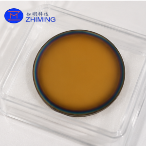
- Ultra-thin diamond layer below 1 μm
- True wafer-level thermal integration
- Exceptional heat spreading performance
- Compatible with semiconductor manufacturing flows
- Supports high-power and high-frequency device platforms
- Scalable production from 4” to 8” wafers
- Custom engineering and process optimization available
Veelgestelde vragen (FAQ)
What is the main advantage of silicon-integrated diamond film?
It enables heat to be dissipated directly at the wafer level, reducing thermal resistance at the source and improving device performance and reliability.
Can it be integrated into existing semiconductor processes?
Yes. The film is designed to be compatible with standard silicon wafer manufacturing and can be incorporated into existing process flows.
What wafer sizes are supported?
The material is available on 4-inch, 6-inch, and 8-inch silicon wafers, with customization options available for specific applications.
Beoordelingen
Er zijn nog geen beoordelingen.