
Semiconductor manufacturing consumes far more wafers than the wafers that eventually become sellable semiconductor devices.
Before a production wafer enters a new process chamber, engineers may need wafers to verify equipment operation, stabilize a process, measure film uniformity, evaluate contamination, test a new recipe or qualify a newly installed tool.
Using prime-grade production wafers for every one of these tasks would significantly increase operating cost.
For this reason, semiconductor fabs, equipment manufacturers, research laboratories and process-development teams commonly use wafers described as:
- dummy wafers
- reclaim wafers
- test wafers
- monitor wafers
These terms are sometimes used interchangeably, but they do not mean exactly the same thing.
The most important distinction is that dummy wafer and test wafer generally describe how a wafer is used, while reclaim wafer describes how a wafer has been recovered and prepared for reuse.
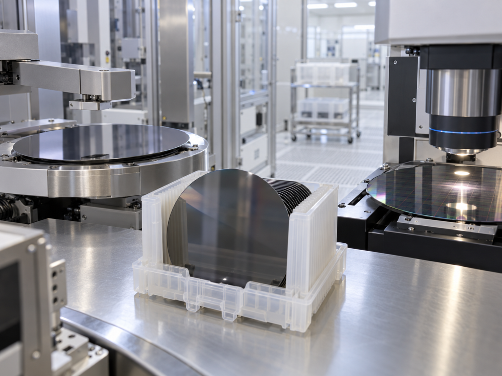
A reclaimed silicon wafer can therefore become a dummy wafer, test wafer or process-monitor wafer depending on its final application.
Understanding these differences helps engineers select a wafer that meets process requirements without unnecessarily paying for production-grade material.
What Is a Dummy Wafer?
A dummy wafer is generally a non-product wafer used to support semiconductor equipment operation, process preparation, equipment testing or manufacturing control.
Unlike production wafers, dummy wafers are not intended to become finished semiconductor devices.
They may be used before or between production lots for activities such as:
- equipment setup
- conditionnement de la chambre
- process stabilization
- qualification des équipements
- recipe development
- mechanical wafer-handling tests
- robot alignment
- temperature stabilization
- deposition conditioning
- cleaning-process development
The required dummy wafer specification depends heavily on the process.
For some equipment-handling tests, the wafer mainly needs to reproduce the dimensions, thickness and mechanical behavior of a production wafer.
For deposition, thermal or plasma processes, surface condition, material, electrical properties and contamination limits can become much more important.
Why Semiconductor Equipment Uses Dummy Wafers
Modern semiconductor equipment is designed around extremely repeatable wafer processing.
Before introducing valuable production wafers, engineers may need to confirm that the tool is operating correctly.
Consider a newly serviced deposition chamber.
Immediately processing production wafers may introduce unnecessary risk if:
- chamber conditions are not yet stable
- robot alignment has changed
- temperature uniformity has shifted
- residual contamination remains
- deposition rate has not stabilized
Dummy wafers provide a lower-cost substrate for these preliminary operations.
They can also be used to establish repeatable chamber conditions after:
- preventive maintenance
- chamber cleaning
- component replacement
- prolonged tool shutdown
- process-recipe modification
The exact procedure is tool- and process-specific.
What Is a Reclaim Wafer?
A reclaim wafer is a previously used wafer that has been processed to remove earlier films, residues or device structures and restore the surface for another use.
For silicon wafers, reclamation may involve several steps such as:
- incoming wafer inspection
- film or coating removal
- surface stripping
- grinding when necessary
- polissage
- chemical cleaning
- dimensional inspection
- surface inspection
- final cleaning and packaging
The objective is not necessarily to return the wafer to exactly the same condition as a new prime wafer.
Instead, the reclaim process prepares the wafer to meet specifications appropriate for its next application.
SUMCO describes reclaimed polished wafers as used wafers from which customer device layers are removed before the wafers are polished and recycled for reuse.
Reclaim Wafer Does Not Automatically Mean Low Quality
A common misunderstanding is that a reclaim wafer simply means a defective or low-quality wafer.
That is not an accurate way to evaluate it.
A reclaimed wafer can be carefully processed, polished, cleaned and inspected.
Its suitability depends on:
- remaining wafer thickness
- TTV
- bow and warp
- surface roughness
- particle level
- metallic contamination
- edge condition
- number of previous reclaim cycles
- intended application
For many equipment qualification and process-development tasks, a properly specified reclaimed wafer may provide all the performance required.
The key is matching the reclaim specification to the process.
Why Reclaim Wafers Are Economically Important
Prime semiconductor wafers can represent unnecessary cost when the wafer itself will not become part of a saleable device.
This becomes increasingly important as wafer diameter, material complexity and substrate cost increase.
Reclaimed wafers can extend the useful life of a substrate by allowing it to be used again for non-product applications.
Typical uses include:
- process testing
- qualification des équipements
- monitor applications
- deposition tests
- cleaning tests
- CMP development
- metrology
- handling tests
Reclaim is therefore both a cost-management strategy and a way of extending wafer utilization.
The concept is particularly attractive for expensive substrate materials when surface restoration is technically and economically practical.
For example, reclaimed SiC wafers are offered specifically for test, monitor, dummy and process-development applications where production-grade material is not required.
What Is a Test Wafer?
A test wafer is a wafer used to obtain information about a semiconductor process, material, piece of equipment or manufacturing condition.
This is a broad functional category.
A test wafer may be used to evaluate:
- deposition thickness
- film uniformity
- etch rate
- etch selectivity
- particle contamination
- plasma uniformity
- CMP removal rate
- oxidation behavior
- thermal uniformity
- lithography performance
- equipment repeatability
- wafer handling
- bonding conditions
- cleaning efficiency
Unlike the term reclaim wafer, “test wafer” does not necessarily tell the buyer whether the wafer is new or reclaimed.
A test wafer may be:
- a new virgin wafer
- a test-grade silicon wafer
- a reclaimed wafer
- an oxide-coated wafer
- a metal-coated wafer
- a patterned wafer
- an epitaxial wafer
- another specially prepared substrate
The wafer specification is determined by what engineers want to measure.
Test Wafer vs Monitor Wafer
Test wafer and monitor wafer are also closely related terms.
A plaquette de test is commonly associated with experiments, qualification or process development.
A monitor wafer is more often associated with measuring and controlling an existing production process.
For example, monitor wafers may be introduced at defined intervals to evaluate:
- film thickness
- uniformity
- particles
- contamination
- etch rate
- process drift
Applied Materials has described the use of blanket monitor wafers for particle inspection and process monitoring, while modern process-control systems increasingly attempt to detect excursions before they affect production yield.
The terminology is not universally standardized in commercial conversations, however.
Some suppliers may classify monitor wafers as a type of test wafer.
For procurement purposes, the actual specification is more important than the name.
Dummy Wafer vs Reclaim Wafer vs Test Wafer
The differences can be summarized as follows:
| Category | Dummy Wafer | Reclaim Wafer | Test Wafer |
|---|---|---|---|
| Main meaning | Application | Wafer condition/source | Application |
| Main purpose | Equipment/process support | Reuse of previously processed wafer | Measurement and evaluation |
| Must be new? | Non | Non | Non |
| Can be reclaimed? | Oui | By definition reclaimed | Oui |
| Used for production devices? | Normally no | Normally non-product applications | Normally no |
| Application type | Conditioning, setup, handling | Lower-cost reuse | Process development and qualification |
| Surface quality required | Application dependent | Application dependent | Test dependent |
| Prime-grade required | Usually not | Non | Sometimes |
| Can carry films? | Oui | After reclaim or further coating | Frequently |
| Main purchasing consideration | Fit for process | Reclaim quality | Measurement objective |
The most important point is that these categories overlap.
Par exemple :
Reclaimed wafer + dummy application
A reclaimed 300mm silicon wafer may be used for chamber conditioning.
Reclaimed wafer + test application
A reclaimed wafer may receive a thermal oxide layer and be used for a deposition experiment.
New wafer + test application
A new virgin wafer may be required when extremely low contamination or precisely controlled electrical characteristics are necessary.
What Is a Virgin Test Wafer?
Not every non-product wafer should be reclaimed.
Some tests require a clean starting substrate with tightly controlled properties.
A virgin test wafer is manufactured from new semiconductor-grade material but may use specifications less restrictive than prime device wafers.
Depending on the application, buyers may specify:
- crystal orientation
- conductivity type
- resistivity
- thickness
- TTV
- bow
- warp
- surface finish
- particle count
- oxide thickness
Virgin test wafers are particularly useful when the experiment depends directly on substrate properties.
Par exemple :
- oxidation studies
- diffusion experiments
- epitaxial growth
- contamination analysis
- electrical characterization
- thin-film research
In these cases, uncertainty from a previous process history may be unacceptable.
Dummy Wafers for Equipment Qualification
Equipment qualification is one of the most important dummy-wafer applications.
When new semiconductor equipment is installed, engineers must demonstrate that the system can operate within required process specifications.
Qualification may involve multiple stages.
Mechanical Qualification
Wafers can be used to verify:
- cassette loading
- FOUP handling
- robot transfer
- wafer centering
- notch recognition
- load-lock operation
- chuck placement
For purely mechanical qualification, wafer geometry may be more important than electronic quality.
Important parameters can include:
- diameter
- thickness
- edge profile
- bow
- warp
- notch geometry
Process Qualification
Process qualification requires more demanding wafer control.
A wafer may be processed through the equipment and measured afterward.
For a deposition tool, engineers might evaluate:
- average film thickness
- within-wafer uniformity
- wafer-to-wafer uniformity
- particle generation
- edge exclusion
For an etch tool, the important characteristics may include:
- etch depth
- etch rate
- selectivity
- uniformity
- surface morphology
In such cases, the wafer becomes both a process vehicle and a measurement substrate.
This type of wafer may reasonably be called a test wafer or monitor wafer rather than simply a dummy wafer.
Dummy Wafers for Chamber Conditioning
Many semiconductor processes are sensitive to the condition of the internal chamber surfaces.
Following maintenance or cleaning, the chamber surface may not behave exactly as it does during steady-state production.
Dummy wafers can be processed to help establish the desired operating condition before product wafers are introduced.
Depending on the process, engineers may run a defined number of non-product wafers while monitoring:
- film thickness
- chamber pressure
- plasma characteristics
- particle performance
- process repeatability
The exact conditioning method must be established for the specific tool and process.
Reclaim Wafers for CMP Development
Chemical mechanical planarization is another application where reclaim wafers can be useful.
CMP engineers may need wafers to evaluate:
- removal rate
- pad behavior
- slurry performance
- surface roughness
- within-wafer uniformity
- scratching
- stabilité du processus
Where the substrate does not need prime device quality, reclaimed wafers can reduce experimental cost.
However, the starting surface must still be sufficiently controlled.
Large variations in:
- TTV
- bow
- surface roughness
- residual film
- contamination
can distort CMP results.
Therefore, reclaimed wafers should still have defined incoming specifications.
Reclaim Wafers for Deposition Testing
Reclaimed silicon wafers are frequently suitable as substrates for evaluating deposition processes.
Possible films include:
- SiO₂
- SiN
- polysilicon
- metals
- dielectric materials
- protective coatings
After deposition, engineers may measure:
- thickness
- uniformity
- stress
- refractive index
- sheet resistance
- particle level
Historically, semiconductor fabs have relied extensively on monitor wafers for measuring film and process behavior, although integrated metrology can reduce the number needed in some processes.
When Should You Use a Dummy Wafer?
Choose a dummy wafer when the primary objective is to support equipment operation rather than create a measurement-standard substrate.
Typical situations include:
Robot and Handler Testing
Use wafers that accurately reproduce the geometry and mechanical characteristics required by the equipment.
Chamber Conditioning
Use non-product wafers capable of tolerating the required process conditions.
Equipment Setup
Use dummy wafers before exposing expensive production wafers to newly adjusted equipment.
Thermal Process Stabilization
Dummy wafers may be used where wafer loading itself affects thermal conditions or equipment behavior.
The required wafer grade can vary significantly between these applications.
When Should You Use a Reclaim Wafer?
Choose a reclaim wafer when:
- virgin wafer quality is unnecessary
- cost reduction is important
- the process can tolerate a previously used substrate
- wafer thickness remains within requirements
- reclaimed surface quality meets the application
Good applications can include:
- equipment testing
- conditionnement de la chambre
- deposition development
- CMP testing
- training
- wafer handling
- process monitoring
The purchaser should specify what the reclaimed wafer needs to accomplish instead of ordering solely by the word “reclaim.”
When Should You Use a Test Wafer?
Choose a test wafer when the primary objective is to generate reliable process data.
Parmi les applications courantes, on peut citer :
- new recipe development
- qualification des équipements
- film-thickness measurement
- process-window characterization
- etch-rate measurement
- particle monitoring
- contamination studies
- lithography evaluation
- experimental semiconductor processing
Modern semiconductor process development relies heavily on metrology and defect inspection to characterize process windows and detect yield-limiting defects before high-volume manufacturing.
The test wafer should therefore be selected according to the parameter being measured.
Silicon Dummy and Reclaim Wafer Specifications
When purchasing silicon dummy or reclaim wafers, several specifications should be considered.
Diamètre de la plaquette
Common sizes include:
- 100mm / 4 inch
- 125mm / 5 inch
- 150mm / 6 inch
- 200mm / 8 inch
- 300mm / 12 inch
Equipment qualification generally requires the same diameter as the production line.
Épaisseur
Thickness can be particularly important for robotic handling and chuck compatibility.
Reclaimed wafers gradually lose material during repeated stripping and polishing.
Therefore, a reclaim wafer may become thinner after each recovery cycle.
Minimum acceptable thickness should be specified.
TTV
Total Thickness Variation affects how consistently the wafer sits on:
- vacuum chucks
- electrostatic chucks
- metrology stages
- CMP equipment
Tighter TTV may be required for precision process-development applications.
Bow and Warp
Excessive bow or warp can interfere with:
- robotic handling
- wafer mapping
- chucking
- lithography
- bonding
- thickness measurement
Mechanical handling applications may therefore require defined bow and warp limits even when the wafer is not prime grade.
Rugosité de surface
Surface requirements vary by application.
For basic mechanical testing, an ultra-smooth surface may not be necessary.
For deposition, bonding or surface-metrology studies, polished surface quality becomes much more important.
Resistivity and Conductivity Type
Some dummy-wafer applications do not care whether the silicon wafer is:
- P-type
- Type N
or what its resistivity is.
Other semiconductor processes are sensitive to electrical properties.
Plasma behavior, electrostatic chuck performance or electrical testing may require controlled resistivity.
Therefore, electrical specifications should only be relaxed when the process genuinely does not depend on them.
Orientation des cristaux
Common silicon wafer orientations include:
- <100>
- <111>
For purely mechanical handling tests, orientation may have limited importance.
For oxidation, etching, device experiments and other material-dependent processes, crystal orientation can significantly affect results.
Surface Oxide and Film Options
Test wafers may also be supplied with controlled films.
Par exemple :
- thermal oxide
- PECVD oxide
- silicon nitride
- polysilicon
- aluminum
- copper
- other metal films
This allows engineers to purchase wafers closer to the actual process condition being evaluated.
What About SiC Dummy Wafers?
As SiC device manufacturing expands, the demand for SiC process and dummy wafers is also increasing.
Using prime SiC substrates purely for:
- equipment setup
- handling qualification
- process development
- monitor applications
can be expensive.
Lower-grade or reclaimed SiC wafers may therefore be attractive for suitable non-device applications.
However, SiC reclaim is more challenging than conventional silicon reclaim because of:
- extreme hardness
- polishing difficulty
- high substrate value
- surface damage control
- tighter thickness economics
Commercial SiC reclaim services specifically position restored wafers for dummy, monitor, test and process-development applications rather than final device fabrication.
Dummy Grade vs Prime Grade
A dummy-grade wafer should not simply be understood as “bad prime wafer.”
The two products are optimized for different purposes.
Prime wafers may require stringent control over:
- crystal defects
- COP
- particles
- metallic contamination
- resistivity
- surface quality
- flatness
- epitaxial suitability
A dummy wafer used for equipment handling may not require many of these specifications.
Relaxing irrelevant specifications lowers cost without necessarily affecting the intended application.
The key is knowing which specifications can safely be relaxed.
How to Select Between Dummy, Reclaim and Test Wafers
A practical selection process can start with the following questions.
1. What Is the Wafer Being Used For?
Is the goal:
- robot testing?
- equipment qualification?
- deposition monitoring?
- CMP development?
- contamination analysis?
- chamber conditioning?
This is the most important question.
2. Does the Wafer Need a Known Process History?
If the experiment is highly sensitive to contamination or surface chemistry, a virgin wafer may be preferable.
If the wafer is only being used as a mechanical process vehicle, reclaim may be perfectly adequate.
3. Is Surface Quality Important?
Processes involving:
- deposition
- bonding
- surface inspection
- optical metrology
generally require tighter surface specifications.
4. Is Thickness Critical?
For equipment handling, wafer thickness may directly affect robot and chuck operation.
Reclaim wafers should therefore be checked for remaining thickness.
5. Is Electrical Resistivity Important?
For certain plasma, electrostatic or electrical experiments, yes.
For many basic mechanical handling tests, perhaps not.
6. How Many Process Cycles Are Required?
High-volume equipment qualification can consume many wafers.
In these applications, reclaim wafers may offer a substantial economic advantage.
Recommended RFQ Information
When requesting dummy, reclaim or test wafers, provide more than just the wafer diameter.
A useful RFQ should include:
Material:
Silicon, SiC or another substrate
Diameter:
100mm, 150mm, 200mm, 300mm, etc.
Thickness:
Nominal thickness and tolerance
Orientation:
<100>, <111>, 4H-SiC (0001), etc.
Conductivity type:
P-type, N-type or not critical
Resistivity:
Required range or “not critical”
Surface:
SSP or DSP
Surface finish:
Polished, etched or application-specific
TTV:
Maximum acceptable value
Bow / Warp:
Maximum values if required
Particle requirement:
Specify if the wafer will be used for contamination-sensitive processes
Application:
Equipment qualification, deposition test, CMP, handling, cleaning, chamber seasoning, etc.
Specifying the intended application is often particularly helpful because it allows the wafer supplier to recommend a suitable grade without over-specifying unnecessary parameters.
A Practical Selection Example
Consider a 300mm deposition equipment manufacturer preparing a new chamber.
For initial robot transfer and wafer mapping:
Dummy wafer
A mechanically representative wafer may be sufficient.
For chamber conditioning:
Reclaimed dummy wafer
A lower-cost reclaimed wafer may provide suitable material for repeated process cycles.
For measuring deposited film uniformity:
Test or monitor wafer
The wafer should have controlled surface quality suitable for thickness and uniformity measurements.
For ultra-low contamination qualification:
Virgin test wafer
A new wafer with a documented surface and contamination specification may be required.
The same equipment qualification program can therefore use several wafer grades.
This illustrates why “dummy,” “reclaim” and “test” should not be treated as mutually exclusive material grades.
Conclusion
Dummy wafers, reclaim wafers and test wafers all reduce the need to consume expensive production wafers during semiconductor equipment qualification and process development, but they describe different aspects of wafer use.
A plaquette factice is primarily a non-product wafer used to support equipment operation, conditioning or process setup.
A reclaim wafer is a previously processed wafer that has been stripped, polished, cleaned and prepared for reuse.
A plaquette de test is selected specifically to generate information about a process, material or piece of semiconductor equipment.
These categories can overlap.
A reclaimed silicon wafer may become a dummy wafer for chamber conditioning today and, after appropriate preparation, serve as a test or monitor wafer in another application.
The best wafer is therefore not always the highest-grade wafer.
The correct choice is the lowest-cost wafer that still controls every parameter that matters to the intended semiconductor process.
For equipment qualification, process development and manufacturing monitoring, careful selection of wafer diameter, thickness, TTV, bow, warp, surface condition, resistivity and contamination level can reduce operating cost while maintaining reliable process data.