
Semiconductor epitaxy refers to the process of growing single-crystal thin films on silicon or silicon carbide (SiC) substrates. The epitaxial layer shares the same crystal orientation as the substrate and can be grown using either the same material (homoepitaxy) or different materials (heteroepitaxy). For high-frequency and high-power devices, epitaxial growth helps optimize device performance: high-resistivity epitaxial layers provide high breakdown voltage, while low-resistivity substrates reduce series resistance, lowering saturation voltage. Epitaxial layers can be doped as P-type or N-type, forming PN junctions that allow unidirectional current flow, enabling rectification. SiC epitaxy is widely applied in power electronics, radio-frequency (RF) devices, and optoelectronic applications.
1. SiC Industry Chain and Value Distribution
The SiC device industry chain consists of three main segments: substrate, epitaxy, and device manufacturing (design, fabrication, and packaging). The substrate and epitaxy stages account for approximately 70% of the value chain, while downstream device processing represents only 30%. This contrasts with conventional silicon devices, where post-wafer processing accounts for most production costs. The high value concentration upstream highlights the strategic importance of substrate and epitaxy technologies.
Substrate segment involves crystal growth, wafer slicing, grinding, and polishing. Crystal growth can be achieved through Physical Vapor Transport (PVT), High-Temperature Chemical Vapor Deposition (HTCVD), or Liquid Phase Epitaxy (LPE). Wafer slicing uses wire saws, diamond wire, laser, or cold separation methods, while chemical mechanical polishing (CMP) ensures flat, defect-free surfaces suitable for epitaxial growth.
2. SiC Substrate Production Process
- Crystal Growth:
- PVT: The mainstream method for SiC crystal growth. Equipment is relatively simple, operating costs are low, and process control is straightforward.
- HTCVD: Produces high-purity crystals but has slower growth rates, lower yields, and higher costs.
- LPE: Produces high-quality, low-defect crystals but growth rate and size are limited.
- Wafer Slicing:
- Wire saws: Standard method with high yield and low cost.
- Diamond wire & laser slicing: Offer higher efficiency, reduced material loss, and environmental benefits.
- Cold separation: Uses internal material stress to separate wafers with minimal loss.
- Grinding and Polishing:
- CMP: The main method for achieving highly flat, defect-free wafer surfaces, critical for high-quality epitaxy.
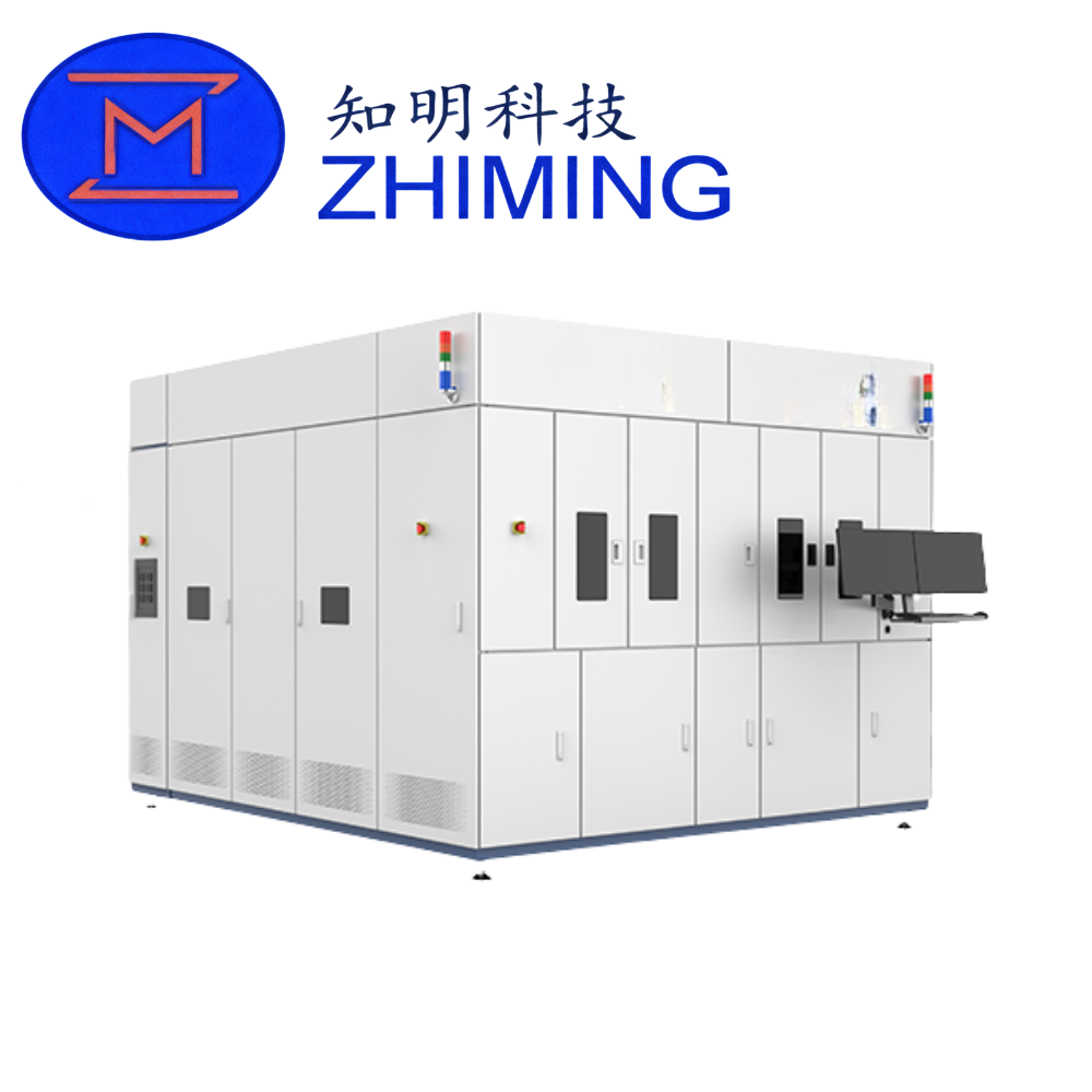
3. Epitaxy Processes and Equipment
Epitaxial growth is a critical step in SiC device fabrication. Unlike conventional silicon devices, SiC devices cannot be processed directly on the substrate. A high-quality single-crystal epitaxial layer must be grown on the substrate before device fabrication.
- Epitaxy Types:
- Homoepitaxy: Growing SiC on conductive SiC substrates, used for low-power devices, RF, and optoelectronic applications.
- Heteroepitaxy: Growing GaN on semi-insulating SiC substrates, used for high-power devices.
- Epitaxy Equipment:
- CVD (Chemical Vapor Deposition): Gaseous precursors react on heated SiC substrates to deposit epitaxial layers.
- MOCVD (Metal-Organic CVD): Uses metal-organic precursors, allowing lower temperature deposition and ultra-thin layers for complex structures.
- LPE: Dissolves source materials in a molten metal solvent and deposits them onto the substrate upon cooling.
- MBE (Molecular Beam Epitaxy): Deposits atomic layers under ultra-high vacuum for precise control over film thickness and composition.
- Post-Epitaxy Wafer Dicing:
- Mechanical dicing and Laser-Dicing are common.
- Laser dicing focuses high-energy pulses on small areas to sublimate or modify material, reducing kerf loss and crack formation.
4. Market and Technology Trends
SiC epitaxy and substrate production remain technology-intensive sectors in the global semiconductor industry. Future trends include:
- Increasing substrate size from 6-inch to 8-inch or larger to reduce unit cost.
- Enhancing epitaxy equipment for high precision, low defect density, and atomic-layer control to meet high-power and high-frequency requirements.
- Advancing dicing technologies toward non-contact, low-loss laser and cold separation methods.
- Promoting domestic and global equipment independence, particularly in epitaxy furnaces and high-precision dicing systems.
5. Schlussfolgerung
SiC epitaxy equipment is essential for manufacturing high-power, RF, and optoelectronic devices. The quality of substrates, epitaxial layers, and dicing equipment directly affects device performance and industry competitiveness. With growing demand for high-power devices, continued advancement and localization of epitaxy technology will play an increasingly critical role in the semiconductor value chain.