

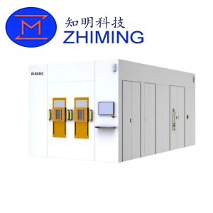
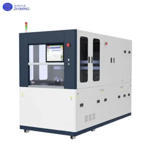
 The Ai80HC (High Beam) Ion Implantation Equipment is a high-current ion implanter specifically designed for 12-inch silicon wafer semiconductor production lines. It is engineered for advanced precision doping processes in modern integrated circuit manufacturing, delivering stable beam performance, high process repeatability, and excellent dose control accuracy.
The system operates within a wide energy range of 0.5 keV to 80 keV, enabling flexible implantation conditions for both shallow and medium-depth junction engineering. It supports multiple implantation species including ¹¹B⁺, ⁴⁹BF₂⁺, ³¹P⁺, ⁷⁵As⁺, ¹⁴N⁺, and ¹H⁺, making it suitable for a wide range of CMOS and advanced logic device fabrication processes.
With an implantation angle range of 0° to 45° and a high angle accuracy of ≤ 0.1°, the system ensures precise control of dopant distribution and junction profile engineering. Combined with beam parallelism of ≤ 0.3° and uniformity of ≤ 1% (1σ), Ai80HC (High Beam) delivers consistent wafer-to-wafer and within-wafer process stability.
Designed for high-efficiency production environments, the system achieves a throughput of ≥ 200 wafers per hour (WPH) while maintaining strict process stability, making it suitable for LSI-compatible advanced semiconductor manufacturing lines.
System Architecture
The Ai80HC adopts a mature and reliable beamline design, consisting of:
- Ion Source
- Extraction System
- Mass Analyzer
- Magnetic Lens System
- Acceleration Tube
- Electrostatic Scanning System
- Parallel Beam Shaping Lens
- Process Chamber (End Station)
- Wafer Cassette / Loader System
It is equipped with:
- Electrostatic wafer chuck stage
- Long-life ion source technology
- Fully automated wafer handling system
This architecture ensures high beam stability, reduced maintenance downtime, and improved process repeatability.
Key Technical Specifications
| Položka | Specifikace |
|---|---|
| Velikost oplatky | 12 inch |
| Energy Range | 0.5 – 80 keV |
| Implanted Elements | ¹¹B⁺, ⁴⁹BF₂⁺, ³¹P⁺, ⁷⁵As⁺, ¹⁴N⁺, ¹H⁺ |
| Implant Angle | 0° – 45° |
| Angle Accuracy | ≤ 0.1° |
| Dose Range | 5E11 – 1E17 ions/cm² |
| Beam Stability | ≤ 10% / hour (within 60 minutes; beam interruption and arcing ≤ 1 time) |
| Beam Parallelism | ≤ 0.3° |
| Throughput (WPH) | ≥ 200 wafers/hour |
| Uniformity (1σ) | ≤ 1% |
| Repeatability (1σ) | ≤ 1% |
| Process Compatibility | Compatible with LSI process |
Klíčové vlastnosti a výhody
1. Intelligent Control System
Equipped with a visualized and intelligent software platform, enabling simplified operation, rapid fault diagnosis, and high system stability during production.
2. Long-Life Ion Source
Adopts advanced ion source design with a lifespan of ≥500 hours, significantly reducing downtime and maintenance cost.
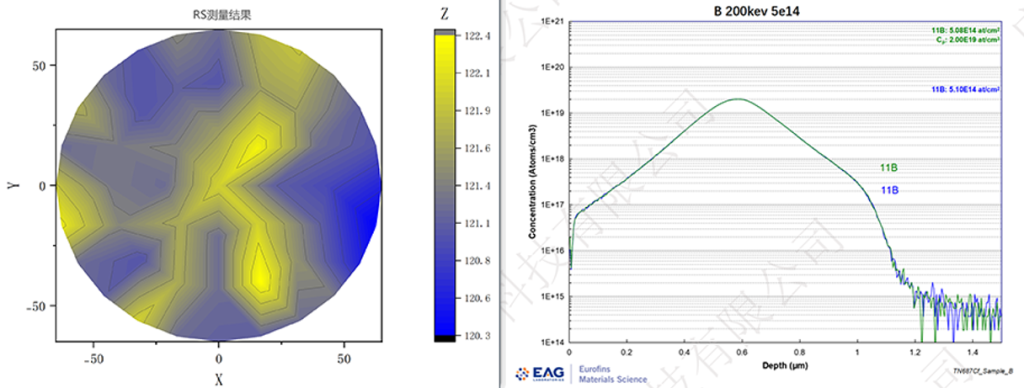
3. Beam Diagnostic Capability
Integrated 2D beam profile measurement system, capable of accurately monitoring:
- Beam width
- Beam height
This improves implantation accuracy and enhances process repeatability.
4. High Production Efficiency
The Ai80HC delivers a throughput performance of more than 1.5× higher than conventional systems, making it suitable for high-volume semiconductor manufacturing environments.
5. Advanced Pattern Implant Function
Supports patterned ion implantation, enabling dose distribution in:
- Circular regions
- Quadrant-based wafer segmentation
This allows:
- Multiple process conditions on a single wafer
- Reduced process development cost
- Improved R&D efficiency
Example: A single wafer can simultaneously receive four different implantation conditions across four quadrants, significantly accelerating process optimization.
Aplikace
- CMOS device fabrication
- Advanced logic IC manufacturing
- Power semiconductor doping
- Research & development semiconductor pilot lines
- Silicon-based integrated circuit production
Často kladené otázky (FAQ)
1. What wafer size is the Ai80HC (High Beam) system designed for?
The Ai80HC (High Beam) ion implantation system is designed for 12-inch silicon wafer production lines, making it suitable for advanced semiconductor manufacturing and high-volume integrated circuit fabrication.
2. What is the energy range and process capability of this system?
The system operates in an energy range of 0.5 keV to 80 keV, supporting both shallow and medium-depth implantation. It is compatible with LSI processes, including shallow junction formation and source/drain engineering in advanced device structures.
3. What level of precision and stability does the system provide?
Ai80HC (High Beam) ensures high process consistency with:
- Angle accuracy ≤ 0.1°
- Uniformity (1σ) ≤ 1%
- Repeatability (1σ) ≤ 1%
- Beam parallelism ≤ 0.3°
These specifications ensure stable wafer-to-wafer performance and high-yield semiconductor production.
Recenze
Zatím zde nejsou žádné recenze.