
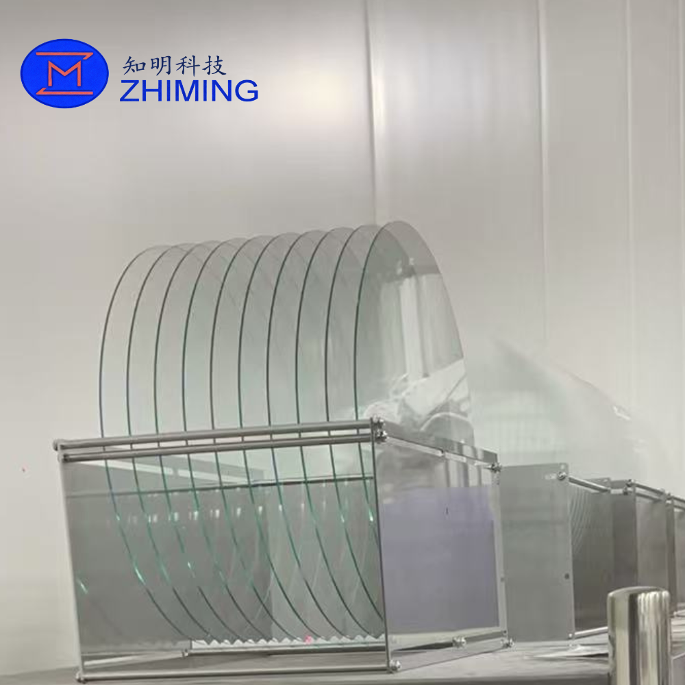
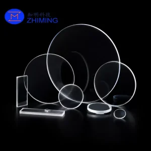
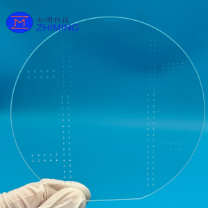
 12palcová (300 mm) skleněná destička je špičkový substrát určený pro pokročilou výrobu polovodičů, MEMS zařízení, optické systémy a balení na úrovni destičky (WLP / FOWLP). Vzhledem k tomu, že se integrace zařízení neustále zvyšuje a struktury balení se stávají složitějšími, stávají se skleněné destičky s velkým průměrem klíčovou alternativou k tradičním křemíkovým substrátům.
Ve srovnání s menšími formáty destiček nabízejí 12palcové skleněné destičky výrazně vyšší výrobní efektivitu, lepší škálovatelnost pro hromadnou výrobu a kompatibilitu s pokročilými litografickými a balicími procesy. Jsou široce využívány v elektronických systémech nové generace, které vyžadují vysokou rozměrovou stabilitu, nízké dielektrické ztráty, vynikající optickou průhlednost a mimořádně hladký povrch.
Tyto destičky se vyrábějí z vysoce čistých materiálů, jako je borosilikátové sklo, tavené křemenné sklo, křemen a sklo bez alkalických prvků, v závislosti na požadavcích dané aplikace. Každá destička prochází procesy přesného řezání, broušení, leštění a čištění, aby byla zajištěna přísná kontrola rovinnosti, rovnoměrnosti tloušťky a drsnosti povrchu.
Dostupné typy materiálů pro 12-palcové skleněné destičky
Borosilikátové sklo (12-palcová destička)
- Vynikající shoda tepelné roztažnosti s křemíkem (~3,2 ppm/K)
- Ideální pro aplikace anodického spojování
- Vysoká chemická odolnost
- Stabilní mechanické vlastnosti při teplotních cyklech
- Široce se používá v MEMS a balicích strukturách
Křemenné sklo (12-palcová destička)
- Mimořádně vysoká optická propustnost (rozsah od UV po IR)
- Velmi nízký obsah nečistot a OH
- Odolnost vůči vysokým teplotám
- Drsnost povrchu až do hodnoty Ra ≤ 0,5 nm
- Vhodné pro optické MEMS a fotoniku
Tavené křemenné sklo (12-palcová destička)
- Extrémně nízká tepelná roztažnost (~0,5 ppm/K)
- Syntetický materiál vysoké čistoty
- Vynikající odolnost proti tepelným šokům
- Optická propustnost >90% (rozsah 200–2000 nm)
- Ideální pro špičkové optické a polovodičové aplikace
Sklo bez obsahu alkálií (12-palcová destička)
- Neobsahuje žádné stopy těžkých kovů (As, Sb, Ba, halogenidy)
- Nízké fluorescenční pozadí
- Vysoká dielektrická stabilita
- Kompatibilní s pokročilými polovodičovými technologiemi
- Vynikající chemická odolnost
Hlavní technické parametry (12-palcová skleněná destička)
Rozměrové parametry
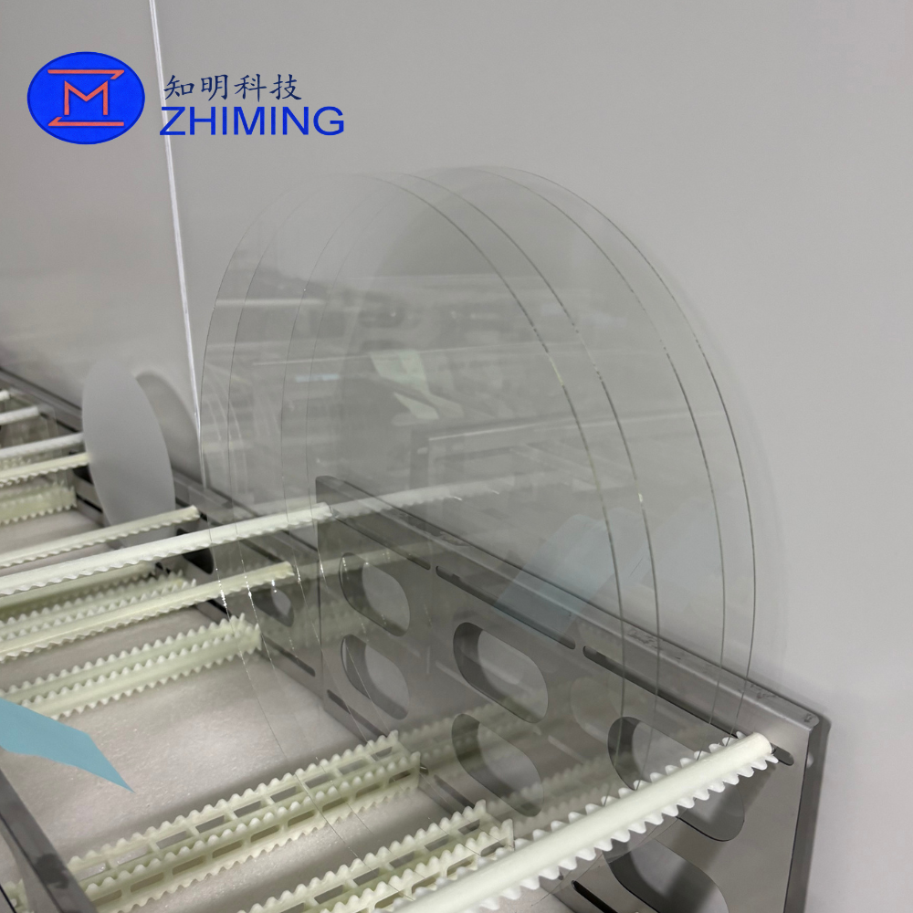
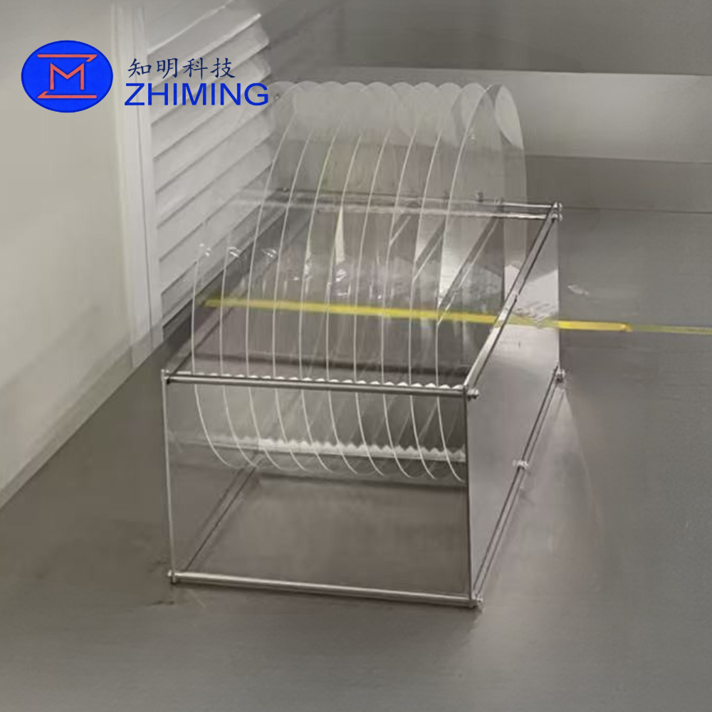
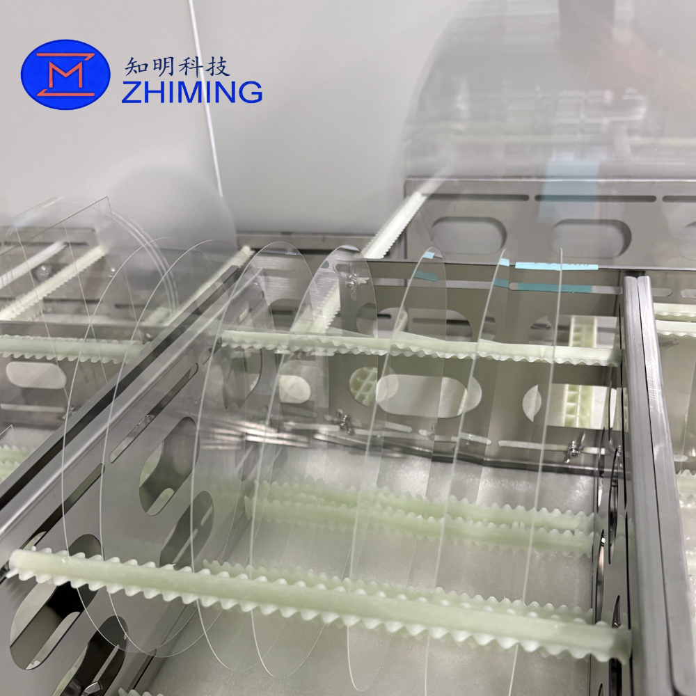
- Průměr destičky: 300 mm (12 palců)
- Rozsah tloušťky: 500 μm – 2000 μm (lze přizpůsobit)
- Tolerance tloušťky: ±5 μm až ±20 μm
- Celková odchylka tloušťky (TTV): ≤ 10–15 μm (vysoce přesná třída)
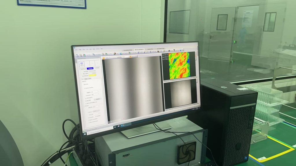
Kvalita povrchu
- Drsnost povrchu (Ra): ≤ 1,0 nm (standard)
- Varianta s ultraleštěným povrchem: Ra ≤ 0,5 nm
- Rovinnost povrchu: ≤ λ/10 (volitelná specifikace pro vysokou kvalitu)
- Zpracování hran: zkosené / zaoblené / profil podle přání
- K dispozici v provedení s oboustranným leštěním (DSP) nebo jednostranným leštěním (SSP)
Vlastnosti materiálu (referenční hodnoty)
| Typ materiálu | CTE (ppm/K) | Převodovka | Hlavní vlastnost |
|---|---|---|---|
| Borosilikát | ~3.2 | Střední | Kompatibilita při lepení křemíku |
| Quartz | ~0.55 | Vysoká (UV–IR) | Výkon na úrovni optických komponentů |
| Tavené křemenné sklo | ~0.5 | >90% | Vysoce čistý a stabilní |
| Sklo bez obsahu alkálií | ~3–4 | N/A | Nízká úroveň znečištění |
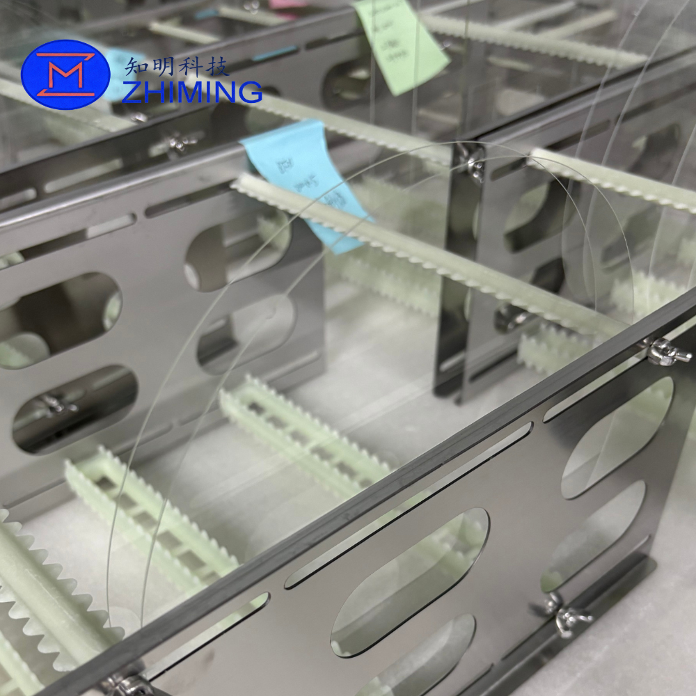
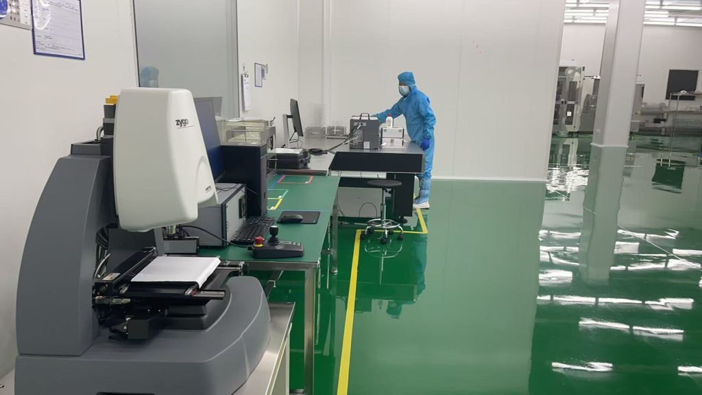
Výrobní kapacity
Naše 12-palcové skleněné destičky se vyrábějí za podmínek pokročilé přesné výroby:
- Vysoce přesné CNC frézování a řezání
- Chemicko-mechanické leštění (CMP)
- Technologie povrchové úpravy v subnanometrovém měřítku
- Čištění a kontrola v čistotě odpovídající standardům čistých prostor
- Kontrola tloušťky a rovinnosti
- Kompatibilita s normami SEMI / JEIDA (v příslušných případech)
Zajišťujeme jak vývoj prototypů, tak i velkosériovou výrobu.
Využití 12-palcových skleněných destiček
12-palcové skleněné destičky se hojně využívají v pokročilých průmyslových odvětvích nové generace:
- Balení polovodičů na úrovni destičky (WLP / FOWLP)
- MEMS senzory a akční členy
- Fotónové integrované obvody (PIC)
- Moduly pro optickou komunikaci
- Pokročilé technologie displejů (OLED / MicroLED)
- Senzorové systémy pro automobilový průmysl (LiDAR, radar, snímání)
- Biočipy a lékařská diagnostická zařízení
- Vysokofrekvenční RF a mikrovlnné součástky
- Přesné optické systémy a litografické platformy
Výhody 12-palcového skleněného plátku
- Plná kompatibilita s výrobními linkami na polovodiče o délce 300 mm
- Vynikající rozměrová stabilita při zpracování velkoplošných materiálů
- Mimořádně nízká drsnost povrchu (<1 nm Ra)
- Vysoká optická průhlednost (v závislosti na typu materiálu)
- Vynikající izolační vlastnosti
- Vysoká chemická a tepelná stabilita
- Vhodné pro výrobní prostředí s velkými objemy výroby
- Možnost přizpůsobení tloušťky, materiálu a povrchové úpravy
FAQ (Často kladené otázky)
Otázka 1: Mohou 12-palcové skleněné destičky nahradit křemíkové destičky v polovodičových aplikacích?
12-palcové skleněné destičky sice nemohou plně nahradit křemíkové destičky při výrobě aktivních prvků, ale jsou široce využívány jako pokročilé substráty nebo nosné materiály v oblasti balení polovodičů, MEMS a fotonických systémů. Skleněné destičky se vyznačují vynikající elektrickou izolací, optickou průhledností a nižšími dielektrickými ztrátami, díky čemuž jsou ideální pro balení na úrovni destičky (WLP), fan-out WLP (FOWLP) a aplikace optické integrace, kde není zapotřebí křemík jako aktivní polovodičová vrstva.
Otázka č. 2: Jaké úrovně rovinnosti a kvality povrchu můžete dosáhnout u 12-palcových skleněných destiček?
U vysoce přesných 12-palcových skleněných destiček dokážeme zajistit mimořádně přísnou kontrolu povrchu. Mezi typické specifikace patří:
- Drsnost povrchu (Ra): ≤ 1,0 nm (standardní kvalita), až ≤ 0,5 nm (ultraleštěná kvalita)
- Celková odchylka tloušťky (TTV): ≤ 10–15 μm v závislosti na materiálu a tloušťce
- Rovinnost povrchu: až do λ/10 (volitelná špičková specifikace)
Tyto parametry zajišťují vynikající kompatibilitu s pokročilými procesy litografie, lepení a nanášení tenkých vrstev.
Otázka č. 3: Lze 12-palcové skleněné destičky přizpůsobit konkrétním aplikacím nebo technologickým požadavkům?
Ano. 12-palcové skleněné destičky lze do značné míry přizpůsobit. Můžeme upravit řadu parametrů podle vašich technologických požadavků, včetně:
- Typ materiálu (borosilikát, křemen, tavený křemen, sklo bez alkalických prvků)
- Tloušťka (od 500 μm do 2 mm nebo více)
- Povrchová úprava (leštění metodou SSP nebo DSP)
- Profil hrany (zkosený, zaoblený nebo vlastní provedení hrany)
- Rovinnost, TTV a stupně drsnosti povrchu
- Speciální vzory, vyrovnávací značky nebo laserové gravírování
Přizpůsobení je obzvláště důležité u MEMS, optických systémů a aplikací v oblasti pokročilých balicích technologií, kde je kompatibilita procesů zásadní.

Recenze
Zatím zde nejsou žádné recenze.