
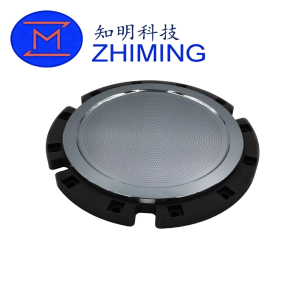
حامل الرقائق المؤقت المصنوع من الياقوت هو ركيزة عالية الأداء مصممة خصيصًا لعمليات التعبئة المتطورة لأشباه الموصلات، ولا سيما لمناولة الرقائق فائقة النحافة وتطبيقات التكامل غير المتجانس.
ويُستخدم على نطاق واسع في تغليف الدوائر المتكاملة ثنائية الأبعاد/ثلاثية الأبعاد (2.5D/3D)، وعمليات التسوية الرأسية (TSV) والتسوية الرأسية المباشرة (RDL)، وتغليف الرقائق/الألواح ذات التوزيع المتفرع (FOWLP/FOPLP)، بالإضافة إلى سير عمل عمليات الربط المؤقت وفك الربط.
تم تصميم الحامل بحيث يتميز بصلابة فائقة واستقرار حراري ممتاز، مما يوفر منصة ميكانيكية دقيقة ومستقرة لعمليات ترقق الرقائق ومعالجة وجهها الخلفي، مما يتيح التعامل بشكل موثوق مع الرقائق التي يقل سمكها عن 50 ميكرومتر مع الحفاظ على سلامة أبعادها في ظل ظروف الدورات الحرارية المعقدة.
 التحديات التي تواجه القطاع
تستمر التغليفات المتطورة في التطور نحو هياكل أرق وأحجام أكبر وكثافة تكامل أعلى. ومع ذلك، لا يزال عدم استقرار العمليات يمثل عقبة رئيسية.
وتشمل التحديات التقنية الرئيسية ما يلي:
- تباين معامل التمدد الحراري (CTE) بين مواد التغليف المتعددة
- تراكم الإجهاد خلال الدورات الحرارية المتكررة
- انكماش المادة اللاصقة أثناء المعالجة والتشوه السطحي
- توزيع غير متجانس للسمك في مجموعات الرقائق فائقة الرقة
- انحراف المحاذاة الناجم عن الالتواء وفقدان الإنتاجية
- الهشاشة الميكانيكية للرقائق فائقة الرقة أثناء المناولة والنقل
تؤثر هذه القضايا بشكل كبير على معدل إنتاجية العمليات وموثوقيتها وقابليتها للتوسع في مجال تصنيع التغليف المتطور.
 الحل: منصة Sapphire Carrier
يوفر الياقوت منصة مادية مثالية لحاملات الرقائق المؤقتة بفضل مزيجه الفريد من القوة الميكانيكية والشفافية البصرية والاستقرار الحراري.
وهي تتيح:
- دعم ميكانيكي عالي الدقة للرقائق فائقة النحافة
- تقليل الانحناء والتشوه أثناء المعالجة
- التوافق مع تقنيات فصل الطبقات باستخدام الليزر
- توزيع متجانس للضغط عبر ركائز واسعة المساحة
- أداء ثابت في البيئات ذات درجات الحرارة المرتفعة والبيئات الكيميائية
المزايا الرئيسية في الأداء
معامل يونغ مرتفع (345–420 جيجاباسكال)
يوفر صلابة استثنائية، مما يحد بشكل فعال من انحناء الرقاقة والتشوه الهيكلي أثناء العمليات الحرارية والميكانيكية.
قوة ميكانيكية عالية (1800–2200 هيرتز)
يضمن مقاومة عالية للتلف السطحي والتآكل الميكانيكي، مما يتيح إعادة استخدامه على المدى الطويل في البيئات الصناعية.
نفاذية ضوئية عالية (>83%، 300–1200 نانومتر)
يتيح نقل الليزر بكفاءة، ويدعم عمليات الفصل بالليزر المتطورة وعمليات الربط المؤقت.
تجانس ممتاز في المواد
يقلل من التباين الموضعي في الضغط عبر حاملات كبيرة الحجم، مما يحسن اتساق العملية واستقرار العائد.
استقرار حراري وكيميائي فائق
يحافظ على سلامة هيكله في ظل التعرض المتكرر للتقلبات الحرارية وعمليات التنظيف الكيميائية.
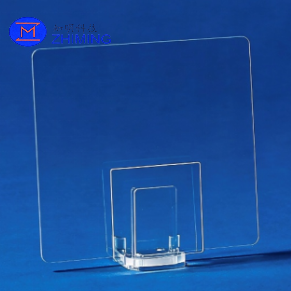
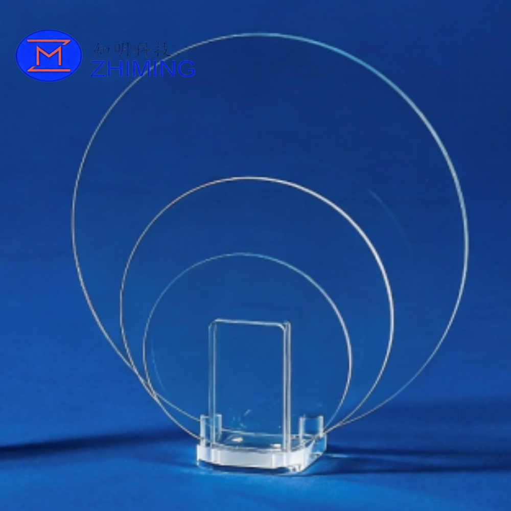
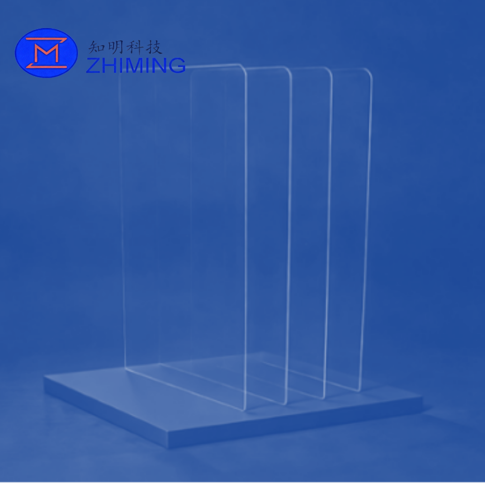
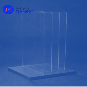
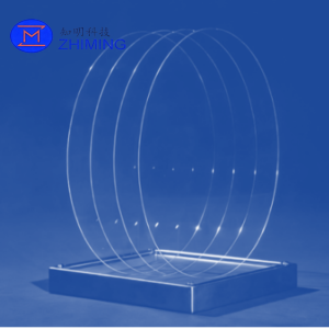
المواصفات الفنية
الهندسة والأشكال
| المعلمة | المواصفات |
|---|---|
| حجم الرقاقة | 8 بوصة / 12 بوصة |
| حجم اللوحة | 100 × 100 مم إلى 510 × 515 مم |
| نطاق السُمك | 0.7 – 2.0 ملم |
الأداء من حيث الأبعاد والسطح
| الممتلكات | الدرجة القياسية | درجة عالية الدقة |
|---|---|---|
| التباين الكلي للسمك (TTV) | ≤ 3 ميكرومتر | ≤ 2 ميكرومتر |
| الاعوجاج | ≤ 100 ميكرومتر | ≤ 50 ميكرومتر |
| تفاوت السماكة | ±0.010 ملم | ±0.005 ملم |
| خشونة السطح (Ra) | < 1.0 نانومتر | < 1.0 نانومتر |
| خدش/حفر | 60/40 | 40/20 |
خواص المواد
| الممتلكات | القيمة |
|---|---|
| معامل يونغ | 345 – 420 جيجاباسكال |
| مقياس صلابة فيكرز | 1800 – 2200 فولت |
| النفاذية الضوئية | >83% (300–1200 نانومتر) |
| الكثافة | 3.98 غ/سم³ |
| التوصيل الحراري | 30–40 واط/م·كلفن |
| CTE (20 درجة مئوية) | 5.6 – 7.7 × 10⁻⁶/كلفن |
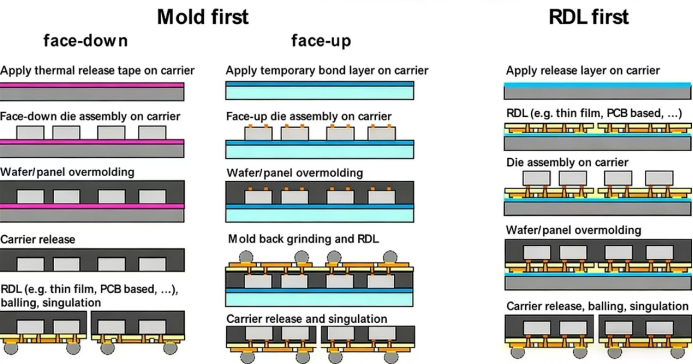
 مجالات التطبيق
- معالجة الجانب الخلفي للرقائق فائقة النحافة
- التكامل غير المتجانس ثنائي الأبعاد ونصف / ثلاثي الأبعاد
- تصنيع ثقوب التوصيل عبر السيليكون (TSV)
- تشكيل طبقة إعادة التوزيع (RDL)
- أنظمة الربط والفك المؤقتة للرقائق
- التغليف على مستوى الرقاقة مع توزيع الأطراف (FOWLP)
- التعبئة على مستوى اللوحة ذات التوزيع الجانبي (FOPLP)
- تقنيات متطورة لتخفيف سماكة الرقائق ومعالجتها (رقائق أقل من 50 ميكرومتر)
القيمة الهندسية
يتيح حامل الرقائق المؤقت المصنوع من الياقوت لشركات تصنيع التغليف المتطور تحقيق ما يلي:
- انخفاض ملحوظ في انحناء الرقاقات والتشوه الهيكلي
- تحسين دقة المحاذاة في عمليات التغليف ذات المسافات الدقيقة
- معالجة مستقرة للرقائق فائقة النحافة التي يقل سمكها عن 50 ميكرومتر
- تحسين ثبات الإنتاجية في التصنيع على نطاق واسع
- تحسين قابلية تكرار العملية واستقرار الإنتاج
- التوافق مع منصات التكامل غير المتجانسة من الجيل التالي
الأسئلة الشائعة
السؤال 1: ما هي الميزة الرئيسية لاستخدام الياقوت في حاملات الرقائق المؤقتة؟
ج: يتميز الياقوت بصلابة فائقة وصلابة عالية واستقرار حراري، مما يتيح تحكمًا فائقًا في الانحناء وموثوقية ميكانيكية عالية في عمليات التغليف المتطورة.
السؤال 2: هل الياقوت مناسب لعمليات الفصل بالليزر؟
ج: نعم. إن نفاذيتها الضوئية العالية عبر الأطوال الموجية من الأشعة فوق البنفسجية إلى الأشعة تحت الحمراء المتوسطة تتيح اختراق الليزر بكفاءة، مما يجعلها متوافقة تمامًا مع أنظمة الفصل بالليزر.
السؤال 3: هل يمكن لحاملات الياقوت أن تدعم تغليف الألواح ذات الحجم الكبير؟
ج: نعم. يمكن تصنيع حاملات الياقوت بأحجام كبيرة مع الحفاظ على استواء ممتاز وتوزيع متجانس للضغط، مما يجعلها مناسبة لتقنية FOPLP وتطبيقات التغليف المتطورة الأخرى ذات المساحات الكبيرة.
المراجعات
لا توجد مراجعات بعد.