
Silicon carbide wafer manufacturing is entering a new stage.
After years of industry transition from 150mm to 200mm substrates, attention is already beginning to turn toward an even larger format: the 300mm SiC wafer.
In January 2026, Wolfspeed announced that it had successfully produced a single-crystal 300mm silicon carbide wafer, describing the development as an important technology milestone toward future scalable SiC platforms.
The announcement does not mean that 300mm SiC has already become a mainstream commercial wafer size. 150mm and 200mm remain much more established.
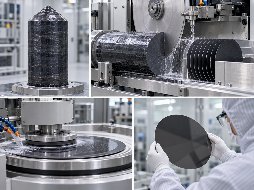
However, the milestone demonstrates that the industry is already exploring the next step in SiC wafer scaling.
Moving from 200mm to 300mm is not simply a matter of producing a larger circle. Every stage—from crystal growth to slicing, grinding, polishing and dicing—becomes more difficult.
Why Move SiC Toward Larger Wafer Diameters?
The motivation is similar to the historical transition from smaller to larger silicon wafers.
A larger wafer provides more surface area, allowing more devices or larger structures to be fabricated during each process cycle.
In principle, this can improve:
- equipment productivity;
- material utilization;
- number of dies per wafer;
- manufacturing scalability;
- compatibility with large-format semiconductor infrastructure.
However, the benefits only become meaningful if wafer quality and manufacturing yield can be maintained.
For silicon carbide, that is particularly challenging.
SiC is one of the hardest semiconductor materials used commercially. Its crystal growth process is complex, and defect control becomes progressively more difficult as boule diameter increases.
Challenge 1: Growing a 300mm SiC Crystal
The manufacturing process begins long before wafer slicing.
Most commercial 4H-SiC substrates are produced using physical vapor transport or related sublimation growth techniques.
Silicon carbide source material is heated to very high temperatures. Vaporized species are transported toward a seed crystal, where a SiC single crystal gradually grows.
Scaling this process to 300mm requires extremely precise control.
Important parameters include:
- temperature distribution;
- axial thermal gradient;
- radial thermal gradient;
- vapor transport;
- crystal interface shape;
- growth rate;
- stress distribution.
As crystal diameter increases, maintaining uniform thermal conditions across the entire growth interface becomes much more difficult.
Small temperature differences can influence crystal quality and defect formation.
Potential defects include:
- micropipes;
- basal plane dislocations;
- threading screw dislocations;
- threading edge dislocations;
- stacking faults;
- polytype inclusions.
Producing a large crystal is therefore only part of the challenge. The entire usable area must also meet acceptable defect specifications.
Challenge 2: Controlling Stress in a Larger Boule
Thermal stress is another major concern.
SiC crystal growth takes place at extremely high temperatures. During cooling, temperature gradients can generate mechanical stress inside the boule.
With increasing diameter, the distance from the center to the edge becomes larger, making uniform cooling more difficult.
Residual stress can later contribute to:
- wafer bow;
- wafer warp;
- cracking;
- slicing instability;
- polishing difficulties.
This means 300mm development requires advances not only in crystal growth equipment but also in thermal-field design and process control.
Challenge 3: Slicing SiC Efficiently
Once a usable boule has been produced, it must be converted into wafers.
This is another difficult step because SiC has a Mohs hardness of approximately 9, making it much harder to machine than silicon.
Traditional wafer slicing methods remove material from the crystal using abrasive cutting.
The objectives include:
- minimizing kerf loss;
- maintaining thickness uniformity;
- reducing subsurface damage;
- controlling bow;
- preventing edge cracking;
- maximizing wafer yield from each boule.
Because high-quality SiC crystal material is valuable, kerf loss is particularly important.
Every micrometer of unnecessary material removal represents lost crystal material.
As wafer diameter increases, the slicing path becomes longer and mechanical stability becomes more demanding.
Wire Saw and Advanced Slicing Technologies
Diamond wire sawing is widely associated with hard-material wafer slicing.
Process variables can include:
- wire speed;
- feed rate;
- diamond abrasive size;
- wire tension;
- coolant or cutting fluid;
- crystal orientation.
Improper control can create surface damage or thickness variation.
The semiconductor industry is also exploring alternative approaches intended to reduce kerf loss and improve SiC material utilization.
Regardless of the technique, scaling toward larger diameters increases the importance of accurate crystal positioning and process stability.
Challenge 4: Wafer Grinding
A freshly sliced SiC wafer cannot normally proceed directly into semiconductor device manufacturing.
Sawing leaves surface irregularities and subsurface mechanical damage.
Grinding is therefore used to improve:
- thickness;
- flatness;
- surface condition;
- parallelism.
Coarse grinding can remove slicing damage relatively quickly, while finer grinding progressively improves the surface.
Because SiC is extremely hard, grinding-wheel selection and process parameters are critical.
Excessive force may produce microcracks or subsurface damage. Insufficient material removal may leave defects that affect later polishing.
For 300mm wafers, uniform pressure distribution becomes even more important.
TTV, Bow and Warp Become Critical
Three parameters are particularly important for large semiconductor wafers:
Total Thickness Variation (TTV)
The difference between the maximum and minimum wafer thickness.
Bow
The deviation of the wafer’s median surface from a reference plane.
Warp
The total deviation of the wafer surface from a reference plane, taking overall deformation into account.
As diameter increases, maintaining tight geometry becomes increasingly difficult.
Even relatively small internal stress or machining non-uniformity can produce measurable deformation across a 300mm substrate.
Poor geometry can create problems during:
- lithography;
- vacuum chucking;
- epitaxial growth;
- wafer transfer;
- bonding;
- automated inspection.
Challenge 5: SiC Polishing
After grinding, SiC wafers typically require precision polishing.
Chemical mechanical polishing is commonly used to achieve the extremely smooth surface required for epitaxial growth and semiconductor processing.
The goal is not simply to make the wafer look visually smooth.
The polished surface must minimize:
- scratches;
- pits;
- residual grinding damage;
- contamination;
- local roughness;
- subsurface defects.
SiC’s chemical stability makes polishing slower and more difficult than silicon.
Large-diameter wafers further increase the challenge of maintaining uniform removal across the entire surface.
Challenge 6: Wafer Dicing
After device fabrication, the wafer must ultimately be separated into individual dies.
Again, SiC hardness creates difficulties.
Mechanical blade dicing can generate:
- edge chipping;
- microcracks;
- kerf loss;
- blade wear.
Laser dicing technologies can offer advantages for certain SiC structures, particularly when narrow kerfs or reduced mechanical force are required.
However, laser processing introduces its own considerations, including:
- heat-affected zones;
- debris;
- laser wavelength;
- focal depth;
- material thickness;
- dicing speed.
The optimal process depends on device structure and wafer specifications.
300mm SiC Could Go Beyond Traditional Power Devices
SiC is best known as a material for high-voltage and high-efficiency power electronics.
Typical applications include:
- electric vehicles;
- charging infrastructure;
- industrial power systems;
- renewable energy;
- high-voltage power conversion.
However, the potential role of large-area SiC may become broader.
In March 2026, Wolfspeed also discussed the possibility of using its 300mm SiC technology platform as a materials foundation for advanced AI and HPC packaging applications, including large interposer concepts.
This remains a forward-looking application rather than a mature high-volume market, but it demonstrates how SiC is being investigated beyond conventional power electronics.
What Does 300mm SiC Mean for the Supply Chain?
If SiC eventually follows silicon toward larger wafer diameters, manufacturing equipment will also need to evolve.
This could affect:
- crystal growth furnaces;
- wire saws;
- grinding equipment;
- polishing equipment;
- wafer carriers;
- vacuum chucks;
- inspection systems;
- laser dicing machines;
- automated wafer handling.
Suppliers will need equipment capable of handling both the increased diameter and the unique mechanical characteristics of SiC.
Consumables such as diamond grinding wheels and wafer dicing blades may also require optimization.
200mm Remains Important
Despite excitement around 300mm technology, it is important to maintain perspective.
A successful 300mm demonstration does not mean the industry will immediately abandon 150mm or 200mm production.
Moving to a new wafer size requires enormous investment in:
- crystal growth;
- substrate manufacturing;
- epitaxy;
- device fabrication;
- metrology;
- wafer handling;
- packaging.
For the foreseeable future, 150mm and especially 200mm SiC are expected to remain central to commercial manufacturing.
The 300mm milestone should therefore be viewed as a sign of the industry’s long-term direction rather than an immediate replacement of today’s manufacturing platforms.
Looking Ahead
The transition from 150mm to 200mm SiC has already demonstrated how difficult substrate scaling can be.
Moving from 200mm to 300mm raises the challenge again.
Crystal growth must become more uniform. Slicing must reduce material loss. Grinding and polishing must control geometry across a much larger surface. Dicing processes must manage an extremely hard and brittle material without sacrificing yield.
The successful demonstration of a single-crystal 300mm SiC wafer in 2026 shows that the technical roadmap is progressing.
But the most important work may now begin.
For the semiconductor materials industry, the race toward larger SiC wafers will depend not on a single breakthrough, but on improvements across the entire manufacturing chain—from crystal growth and wafer slicing to grinding, polishing, inspection and final device processing.