
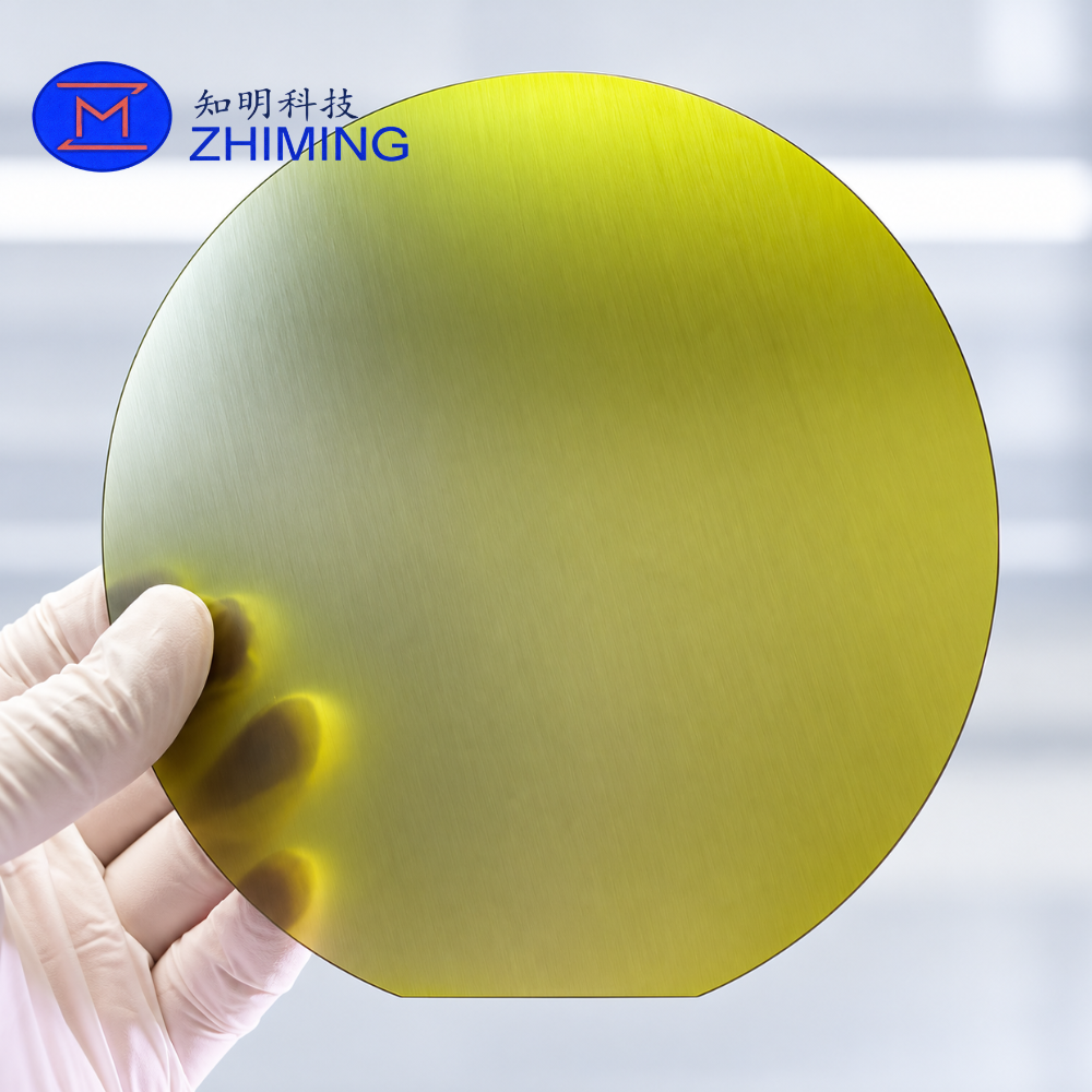
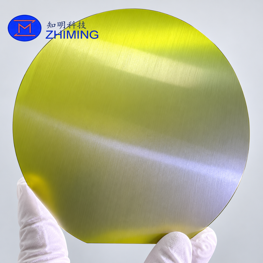
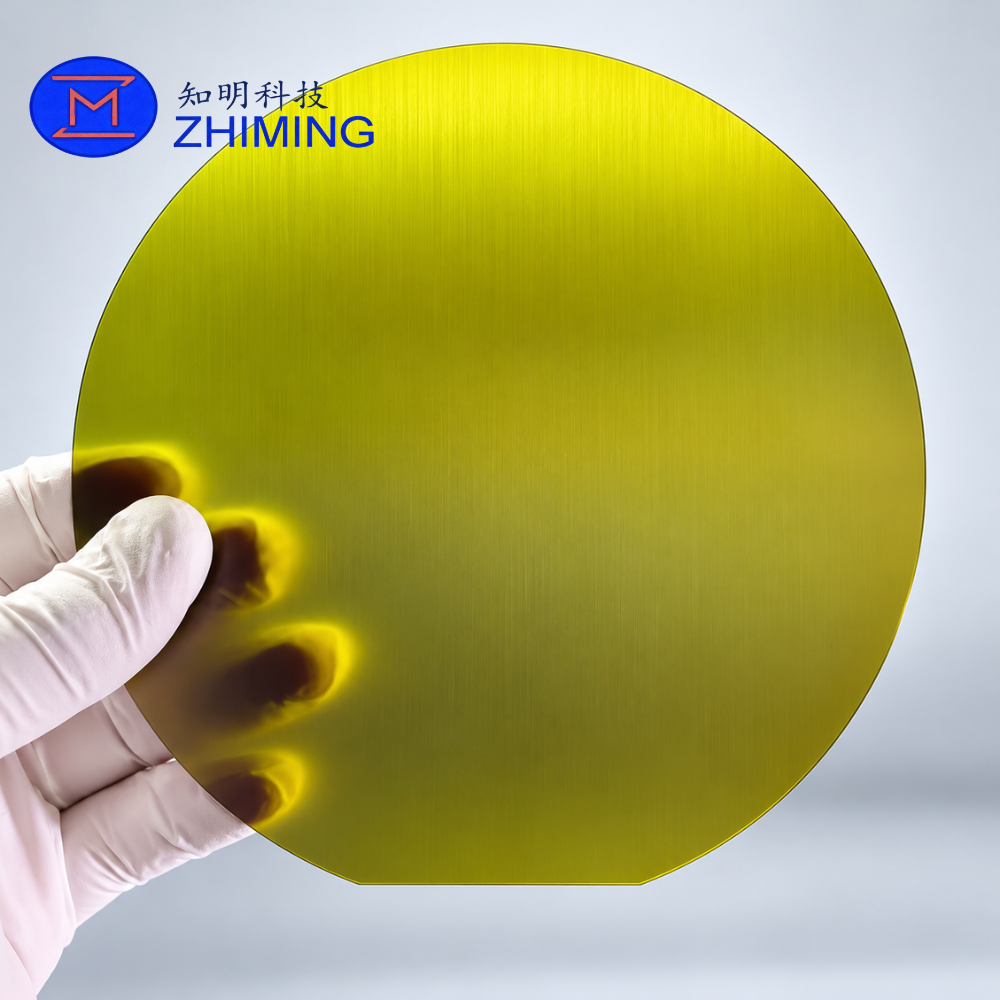
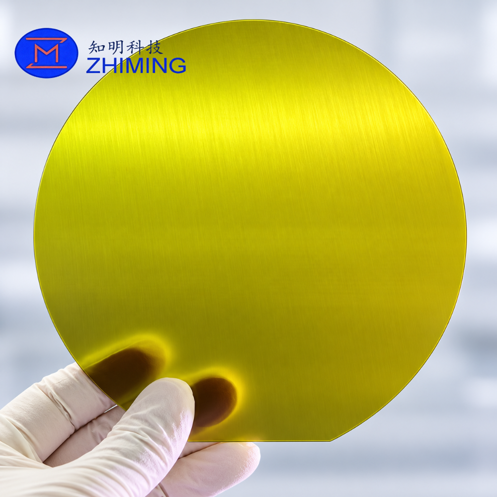
The 6 Inch Raw-Cut SiC Wafers is a silicon carbide wafer supplied directly after crystal slicing, before grinding, lapping, polishing, or CMP treatment.
It is designed for customers who do not require a finished semiconductor-grade polished surface and instead need a cost-effective SiC wafer for machining evaluation, equipment trials, process optimization, surface treatment research, or downstream wafer processing.
The wafer surface may retain visible slicing traces and directional machining marks, which are normal characteristics of the as-cut condition.
We can provide different wafer thicknesses, SiC crystal types, orientations, conductivity types, and processing levels according to customer requirements.
Main Product Characteristics
- Standard 6 inch / 150 mm wafer size
- As-sliced silicon carbide surface
- Unpolished and non-CMP condition
- Suitable for secondary wafer processing
- Custom thickness available
- Multiple SiC material options
- Suitable for R&D and industrial process testing
- Cost-effective alternative to polished SiC wafers
- Small quantity and batch supply available
General Specifications
| Parameter | Available Specification |
|---|---|
| Material | Silicon Carbide |
| Diameter | 150 mm / 6 Inch |
| Wafer Condition | Raw-Cut / As-Sliced |
| Surface Finish | Unpolished |
| Crystal Type | 4H-SiC / 6H-SiC / Customized |
| Conductivity | N-Type / Semi-Insulating / Customized |
| Crystal Orientation | (0001) / Customized |
| Thickness | According to Customer Requirement |
| Wafer Edge | Flat / Notch / Customized |
| Processing Status | Before Grinding / Polishing |
| Order Quantity | Samples to Batch Production |
All parameters can be discussed according to the customer’s actual processing application.
What Is a Raw-Cut SiC Wafer?
A raw-cut SiC wafer is obtained by slicing a silicon carbide crystal boule or ingot into wafer-shaped discs.
At this stage, the wafer has not yet undergone the full substrate finishing process.
A typical SiC wafer production sequence may include:
Crystal Growth → Slicing → Grinding → Lapping → Polishing → CMP → Cleaning
The raw-cut wafer is supplied at the slicing stage, making it suitable for customers who want to perform subsequent processing themselves.
Typical Uses
Wafer Grinding Tests
Suitable for testing grinding machines, grinding wheels, spindle parameters, feed rates, and material removal performance.
Lapping Process Evaluation
Can be used to optimize lapping pressure, slurry selection, abrasive type, removal rate, and surface flatness.
SiC Polishing Development
Provides a practical starting material for developing mechanical polishing and CMP processes.
Equipment Qualification
Suitable for semiconductor equipment manufacturers testing wafer handling, loading, grinding, thinning, polishing, and transfer systems.
Research and Development
Useful for universities, laboratories, research centers, and process engineers studying SiC machining and wafer manufacturing.
Dummy Wafer Applications
Can be used in some non-device applications where a high-cost epi-ready or CMP-polished substrate is unnecessary.
Surface Appearance
Because the wafer is supplied directly after slicing, the surface can show:
- Wire-saw marks
- Directional surface lines
- Matte or semi-matte appearance
- Higher surface roughness than polished wafers
- Natural variation in reflected light
These characteristics are expected for as-cut silicon carbide wafers and do not indicate a polished or epi-ready surface.
If improved surface quality is required, additional grinding, lapping, SSP, DSP, or CMP processing can be supplied separately.
Processing Levels Available
Depending on your project, SiC wafers can be supplied at different processing stages:
Raw-Cut / As-Sliced
For machining tests and further customer processing.
Ground SiC Wafer
For customers requiring improved thickness control and flatter surfaces.
Lapped SiC Wafer
Suitable for intermediate surface-processing applications.
Single-Side Polished SiC Wafer
One polished surface with the opposite side remaining unpolished or processed to a lower finish.
Double-Side Polished SiC Wafer
Both surfaces polished for applications requiring higher flatness and surface quality.
CMP SiC Substrate
Available for higher-end semiconductor and epitaxial applications.
Custom SiC Wafer Supply
We support customized SiC wafer specifications for both R&D and industrial customers.
Available customization may include:
- Diameter
- Thickness
- Thickness tolerance
- Crystal type
- Doping or conductivity
- Orientation
- Off-angle
- Surface condition
- Edge shape
- Flat or notch
- Grinding
- Lapping
- Polishing
- CMP processing
- Special inspection requirements
Customers can provide drawings, target specifications, or intended applications for technical evaluation.
Recommended Applications
This product is particularly suitable for:
- SiC wafer processing companies
- Grinding equipment manufacturers
- Polishing equipment manufacturers
- CMP process developers
- Semiconductor equipment companies
- Universities and research institutes
- Wafer thinning process development
- Abrasive material testing
- Silicon carbide machining studies
- Dummy wafer testing
Why Buy Raw-Cut SiC Wafers?
Raw-cut SiC wafers provide a practical solution when a finished polished substrate is not necessary.
For grinding, lapping, polishing, equipment adjustment, and manufacturing development, using epi-ready wafers can significantly increase test costs.
Raw-cut wafers allow customers to evaluate their processes using actual SiC material while maintaining better control over project costs.
How to Request a Quote
For faster quotation, please provide:
- Required wafer diameter
- Thickness
- Quantity
- SiC polytype
- Conductivity type
- Crystal orientation
- Required surface condition
- Edge configuration
- Application
- Additional tolerance requirements
Our team can recommend a suitable wafer condition based on your intended process.
Request a Quote for 6 Inch Raw-Cut SiC Wafers – Unpolished Silicon Carbide Wafer for Process Testing
Tell us your required specifications, dimensions, quantity, application and technical requirements. You can also provide drawings or additional project information. Our technical team will review your requirements and reply as soon as possible.

Reviews
There are no reviews yet.