
As semiconductor fabs move toward higher levels of automation, wafer handling is no longer simply a matter of moving a substrate from one station to another.
For 300mm wafers, every contact point matters.
A wafer handling stage must support accurate positioning while minimizing backside contamination, particle generation, edge damage, local stress and wafer deformation. It must also work reliably with robotic end effectors, load ports, aligners, inspection modules and process chambers.
For equipment designers, the challenge is therefore not just to build a mechanically precise stage. The stage must function as part of an integrated automated wafer-handling system.
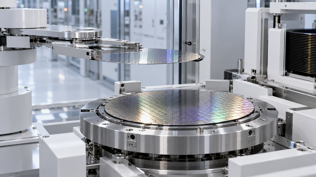
This article examines four of the most important engineering areas:
- Vacuum chuck flatness and support
- Edge-grip wafer handling
- Particle and contamination control
- Robot-to-stage wafer handoff
Why 300mm Wafer Handling Is More Demanding
A 300mm silicon wafer has a large surface area relative to its thickness. Even relatively small mechanical forces, pressure gradients or support errors can produce local deformation.
The challenge becomes more significant when handling:
- Thin wafers
- Back-ground wafers
- Bonded wafers
- Epitaxial wafers
- Patterned device wafers
- Wafers carrying fragile backside structures
- Wafers with strict edge-exclusion requirements
Modern 300mm production lines rely extensively on automated carrier handling and substrate tracking. SEMI’s GEM300 framework covers important functions such as carrier management, substrate tracking and automated process execution in 300mm semiconductor production.
Mechanical interfaces must therefore be designed together with automation requirements rather than as independent components.
1. Vacuum Chuck Flatness Is More Than a Machining Specification
Vacuum chucks are widely used in semiconductor equipment because they provide repeatable wafer positioning without requiring mechanical clamps over the active surface.
Typical applications include:
- Wafer inspection
- Metrology
- Lithography-related positioning
- Grinding
- Polishing
- Dicing
- Coating
- Optical inspection
- Wafer alignment
However, simply machining a chuck to a low flatness value does not guarantee that the wafer will remain flat during operation.
Chuck Surface Geometry
The supporting surface must provide consistent contact across the wafer.
Important parameters include:
Flatness
Large-scale deviation in the chuck surface can transfer directly into wafer deformation.
Local surface variation
A chuck may meet an overall flatness specification while still having localized high points that create stress.
Parallelism
The chuck surface may also need tight parallelism relative to the motion axis, spindle or optical measurement plane.
Surface roughness
An excessively rough surface can increase backside marking or particle trapping, while an extremely smooth continuous surface may create other release or contamination challenges.
The optimum surface therefore depends on the process.
Vacuum Groove Design
Vacuum distribution is equally important.
Common configurations include:
- Concentric grooves
- Radial channels
- Distributed vacuum holes
- Multi-zone vacuum
- Porous vacuum surfaces
The objective is not simply to maximize holding force.
Too much localized vacuum can distort a thin wafer. Poor vacuum distribution can create pressure differences across the substrate. An inappropriate groove pattern can also create unsupported areas.
For thin or temporarily bonded wafers, vacuum pressure often needs to be carefully controlled rather than simply increased.
Material Selection
Wafer stages and chuck components may use materials including:
- Aluminum alloys
- Stainless steel
- Engineering ceramics
- Alumina
- Silicon carbide
- Quartz
- Specialized coated materials
The selection depends on temperature, stiffness, contamination requirements, thermal expansion, vacuum compatibility and machining accuracy.
For precision semiconductor stages, low particle generation and dimensional stability are often as important as mechanical strength.
2. When Edge Grip Is Better Than Backside Vacuum
Vacuum handling is not suitable for every wafer.
In some applications, touching the backside is undesirable or impossible. Examples include wafers with backside films, sensitive structures or contamination restrictions.
This is where edge-contact handling becomes important.
SEMI terminology specifically recognizes an edge contact end effector as an end effector designed to contact a wafer at its edge.
Advantages of Edge Handling
Properly designed edge gripping can:
- Minimize frontside contact
- Reduce backside contact
- Protect sensitive device areas
- Allow handling of certain warped wafers
- Reduce contact with critical surfaces
But the mechanical design becomes more difficult.
Edge Contact Location
The gripping system must remain within an acceptable wafer-edge region.
Engineers must consider:
- Edge exclusion
- Bevel geometry
- Notch position
- Edge profile
- Wafer diameter tolerance
- Grip-pad geometry
The wafer edge is not perfectly rectangular. Semiconductor wafers typically have a shaped edge profile, and the gripping mechanism must accommodate that geometry without creating concentrated stress.
Grip Force
Too little force creates the risk of slippage.
Too much force can result in:
- Edge chipping
- Microcracking
- Local stress
- Particle generation
Grip force should therefore be designed around wafer mass, acceleration, robot motion profile and expected friction rather than using an unnecessarily large safety margin.
Soft Contact Does Not Automatically Mean Clean Contact
Polymer or elastomer contact materials can reduce hard mechanical impact, but they may introduce:
- Wear particles
- Outgassing
- Chemical incompatibility
- Contamination
Material selection must consider the process environment rather than mechanical softness alone.
3. Particle Control Begins With Mechanical Design
A wafer stage can meet all dimensional specifications and still perform poorly in production if it generates particles.
Particles can originate from:
- Sliding contact
- Repeated edge gripping
- Vacuum surfaces
- Robot end effectors
- Bearings
- Cable movement
- Pneumatic mechanisms
- Wafer backside contamination
- Stage coatings
Reduce Sliding Contact
One of the most effective design principles is straightforward:
Avoid dragging the wafer whenever possible.
A wafer should normally be lifted, transferred and placed rather than slid across a support surface.
Even microscopic sliding can release particles or scratch wafer surfaces.
Avoid Particle Traps
Stage geometry should minimize:
- Blind cavities
- Difficult-to-clean grooves
- Exposed fasteners
- Sharp internal corners
- Areas where particles accumulate
Vacuum grooves should also be designed so they can be cleaned without requiring excessive tool disassembly.
Consider Airflow
In atmospheric modules, the stage should not unnecessarily disrupt clean vertical airflow.
Large moving structures can create turbulence and redistribute particles onto the wafer.
For this reason, mechanical design, enclosure geometry and airflow engineering should be evaluated together.
Backside Cleanliness Matters
The backside of a wafer may appear less important than the patterned front surface, but contamination trapped between a wafer and chuck can affect:
- Wafer height
- Local flatness
- Focus
- Metrology accuracy
- Thermal contact
- Particle transfer
In precision optical or dimensional measurement equipment, a single trapped particle can produce a localized wafer-height error.
4. Robot Handoff Is Often the Most Critical Moment
A well-designed chuck and a high-precision robot can still fail if the transition between them is poorly coordinated.
Robot handoff typically involves several steps:
- The end effector approaches the wafer stage.
- The wafer is positioned relative to the stage center.
- The wafer contacts or approaches the support surface.
- Vacuum or another holding method engages.
- The robot releases the wafer.
- The end effector retracts.
Each step creates a potential error source.
SEMI standards for 300mm systems address mechanical interfaces, carriers and transport-module end-effector access because interoperability is fundamental to automated production equipment.
Z-Height Coordination
If the end effector is too high during transfer, the wafer may drop onto the chuck.
If it is too low, the wafer can be forced against the stage or robot blade.
Both conditions can generate particles or damage the edge.
The stage and robot should therefore be calibrated as one mechanical system.
XY Centering
Poor centering may cause:
- Inconsistent chuck support
- Edge sensor errors
- Interference with clamps
- Incorrect process positioning
Pre-aligners or notch alignment systems are often used before precision process placement.
Vacuum Timing
Vacuum timing is frequently overlooked.
If the chuck vacuum engages before the wafer is properly supported, the substrate may be pulled suddenly toward the surface.
If the robot releases too early, the wafer may shift.
A controlled sequence usually requires confirmation signals between:
robot position → wafer presence → stage ready → vacuum established → robot release
Sensor Integration
Useful detection methods may include:
- Vacuum pressure sensing
- Optical wafer-presence sensors
- Capacitive sensing
- Position encoders
- Robot torque feedback
Redundant detection can be valuable in high-value wafer processing because a failed handoff can damage both the wafer and equipment.
5. Designing for Warped and Thin Wafers
Not every 300mm wafer remains perfectly flat.
Wafer deformation may result from:
- Film stress
- Grinding
- Bonding
- Metallization
- Thermal processing
- Temporary adhesives
- Packaging structures
A stage designed only around an ideal flat silicon wafer may have difficulty handling these substrates.
For warped wafers, designers should evaluate:
Capture range
Can the stage establish reliable holding if part of the wafer initially sits above the nominal support plane?
Vacuum zoning
Can vacuum be activated progressively rather than pulling the entire wafer simultaneously?
Edge clearance
Will a bowed wafer collide with the stage or robot during transfer?
Sensor range
Can wafer-presence sensors correctly detect wafers whose vertical position varies?
These considerations become especially important in advanced wafer-level processing.
6. Key Specifications When Designing a Custom Wafer Stage
A useful engineering specification should include more than wafer diameter.
Before designing a 300mm wafer handling stage, define:
| Parameter | Engineering Consideration |
|---|---|
| Wafer diameter | 300mm or other required size |
| Wafer thickness | Standard, thin or back-ground |
| Wafer material | Si, SiC, sapphire, glass or compound semiconductor |
| Surface condition | Bare, polished, patterned, bonded or coated |
| Maximum bow/warp | Determines capture and support strategy |
| Contact area | Backside, edge or non-contact |
| Chuck flatness | Based on process accuracy requirements |
| Vacuum layout | Hole, groove, multi-zone or porous |
| Stage material | Metal, ceramic, SiC, quartz, etc. |
| Motion environment | Static, XY, rotation or high acceleration |
| Temperature | Room temperature or heated/cooled |
| Cleanliness | Cleanroom and process-specific requirement |
| Robot interface | End-effector dimensions and approach geometry |
| Alignment | Notch, edge or vision alignment |
| Sensors | Wafer presence, pressure, position |
| Maintenance | Cleaning and replacement accessibility |
There is no single ideal wafer-stage design for every process.
A stage optimized for optical inspection may be very different from one used for backside grinding, coating or high-temperature processing.
Conclusion
300mm wafer handling stages sit at the intersection of precision mechanics, contamination engineering and factory automation.
Successful designs require more than a flat plate and a vacuum connection.
Engineers must consider the complete wafer-handling sequence:
FOUP → robot → aligner → end effector → wafer stage → process → return transfer
Vacuum chuck geometry affects flatness. Edge-grip geometry affects wafer integrity. Material and contact design influence particle generation. Robot handoff determines whether mechanical precision can be maintained during actual production.
As semiconductor manufacturing becomes increasingly automated, these interfaces become even more important.
For custom wafer handling components, wafer carriers, semiconductor substrates and precision components, equipment designers should specify the wafer type, dimensional requirements, process environment and contact limitations early in the design process. This allows the handling solution to be optimized for both mechanical performance and production reliability.