
Gallium nitride RF devices are commonly grown on substrates such as SiC or silicon.
These platforms have enabled high-performance HEMTs for radar, satellite communication, 5G and RF power amplifiers.
Another substrate is now receiving increasing attention:
bulk single-crystal aluminum nitride — AlN.
Why AlN Is Interesting
AlN has an ultra-wide bandgap of approximately 6 eV.
It also offers high breakdown field, high thermal conductivity, strong chemical stability and close crystal compatibility with III-nitride materials.
For GaN devices, AlN provides a much more closely related crystal platform than conventional silicon.
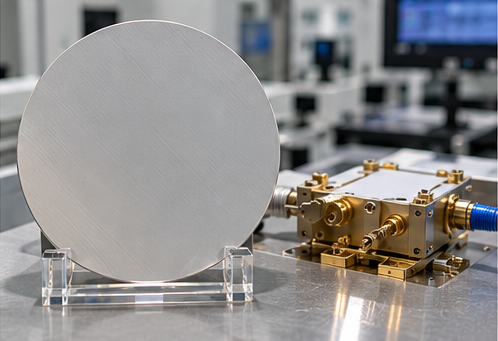
100mm Single-Crystal AlN Changes the Discussion
Historically, one of the main limitations of bulk AlN was wafer diameter.
Small wafers are useful for research but difficult to justify for high-volume semiconductor manufacturing.
The development of 100 mm single-crystal AlN therefore represents an important step toward more practical wafer processing.
Moving Beyond Conventional GaN HEMTs
Emerging structures place GaN channels between wider-bandgap nitride layers.
These architectures may offer stronger confinement and new approaches to high-power RF operation.
A high-quality AlN substrate can provide a suitable foundation for these structures.
Thermal Conductivity Is a Major Advantage
High-power RF transistors generate intense localized heat near the gate region.
If heat is not removed efficiently:
- channel temperature rises;
- mobility decreases;
- reliability degrades;
- output power may need to be reduced.
High-quality AlN offers strong thermal transport and may therefore be attractive for advanced RF architectures.
Direct GaN Growth on Bulk AlN
A key research direction is reducing or eliminating thick intermediate buffer layers.
Even if a bulk substrate has high thermal conductivity, a low-conductivity buffer can become a thermal bottleneck.
Simplified epitaxial stacks may therefore improve heat extraction.
Defect Density Matters
Important AlN wafer parameters include:
- dislocation density;
- orientation;
- surface roughness;
- subsurface damage;
- resistivity;
- Bow;
- Warp.
The surface must also be prepared correctly for subsequent III-nitride epitaxy.
Where AlN Could Fit
Single-crystal AlN is unlikely to replace every GaN-on-SiC or GaN-on-Si application.
It may first serve applications where very high RF power density, high temperature and reduced buffer thermal resistance justify the higher substrate cost.
Conclusion
Single-crystal AlN is moving from a small research crystal toward a genuine semiconductor substrate platform.
The development of larger wafers is making the material increasingly relevant for next-generation RF electronics.
The main challenge now is:
wafer-scale consistency + defect control + acceptable manufacturing cost.