
Silicon photonics has spent many years moving from research laboratories into commercial optical transceivers.
In 2026, the technology is entering another important stage:
300 mm volume manufacturing for AI optical interconnects.
The shift is driven by a fundamental challenge inside AI data centers.
Modern accelerators can process enormous amounts of data, but moving that data between GPUs, switches and racks consumes increasing power.
Electrical copper links become more difficult to scale as bandwidth and distance increase.
Silicon photonics moves part of this communication from electrical signals to light.
That makes the SOI substrate increasingly important.
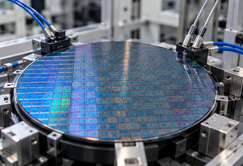
Why SOI Is Important
A Photonics-SOI wafer generally consists of:
top silicon device layer
↓
buried oxide — BOX
↓
silicon handle wafer
The high-index silicon layer forms optical waveguides.
The lower-index buried oxide helps confine light inside the top silicon.
This enables compact photonic structures including:
- waveguides;
- ring resonators;
- Mach-Zehnder modulators;
- grating couplers;
- optical splitters.
Why 220 nm Silicon Is Common
Many silicon-photonics platforms use a top silicon layer around 220 nm.
This thickness provides strong optical confinement at telecom wavelengths while remaining compatible with compact waveguide structures.
But “220 nm” is only a nominal value.
Thickness uniformity across the wafer matters because waveguide geometry influences refractive index, resonance wavelength and coupling efficiency.
Device-Layer Uniformity Becomes a Yield Parameter
A ring resonator designed for one thickness may shift in wavelength if the silicon layer changes across the wafer.
Grating couplers and modulators can also be sensitive to layer thickness and etch depth.
Photonics-grade SOI therefore needs tighter thickness control than many generic SOI applications.
BOX Thickness Also Matters
The buried oxide separates the optical silicon layer from the handle wafer.
If the BOX is too thin, the optical mode may interact more strongly with the handle wafer.
A thicker BOX improves optical isolation.
However, SiO₂ has relatively low thermal conductivity, so thicker BOX may increase thermal resistance.
The correct SOI architecture therefore depends on the device design.
Why 300mm Changes the Manufacturing Equation
Moving to 300 mm allows photonic devices to use mainstream semiconductor infrastructure.
Benefits can include:
- more dies per wafer;
- automated wafer handling;
- mature metrology;
- advanced lithography;
- integration with electronic IC processes.
Wafer Geometry Still Matters
Important parameters include:
- TTV;
- Bow;
- Warp;
- particles;
- surface defects;
- edge profile.
Excessive wafer deformation can affect lithography focus, bonding and automated handling.
CPO Is Raising the Stakes
Co-packaged optics places optical engines much closer to switching or computing ASICs.
This reduces the distance that extremely high-speed electrical signals need to travel.
However, it also creates tighter integration between photonic die, electronic die, package, optical coupling and thermal management.
What Buyers Should Specify
A Photonics-SOI specification may include:
- wafer diameter;
- device-layer thickness;
- device-layer uniformity;
- BOX thickness;
- handle thickness;
- orientation;
- resistivity;
- TTV;
- Bow;
- Warp;
- particles.
Conclusion
Silicon photonics is moving from a device-performance race toward an industrialization race.
AI data centers need optical links that are not only fast but manufacturable at very large scale.
That is why 300 mm Photonics-SOI matters.