
For decades, silicon carbide has been discussed primarily as a semiconductor material for power electronics.
Its wide bandgap, high breakdown field, high-temperature capability and high thermal conductivity have made SiC an important material for:
- electric vehicles;
- charging infrastructure;
- industrial power conversion;
- renewable energy;
- aerospace;
- and high-voltage power devices.
But in 2026, another SiC application is beginning to attract serious attention:
AI and high-performance-computing thermal management.
The reason is simple.
AI processors are becoming extraordinarily powerful, but that power also produces extraordinary amounts of heat.
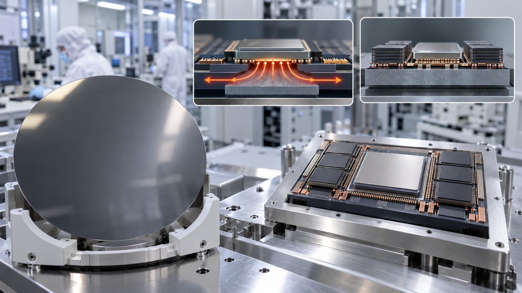
As GPU, HBM and chiplet packages become larger and more densely integrated, removing heat from the package is becoming one of the most important constraints on future AI performance.
This is creating interest in materials that can spread heat more efficiently while remaining mechanically stable and compatible with semiconductor manufacturing.
Single-crystal silicon carbide is emerging as one possible solution.
In March 2026, Wolfspeed announced that its 300 mm SiC technology platform was being explored as a materials foundation for future AI and HPC heterogeneous packaging, highlighting thermal conductivity, mechanical strength and electrical properties.
Then, in August 2026, Coherent announced that it had begun supplying 300 mm high-thermal-conductivity SiC substrate samples to AI semiconductor customers for evaluation in next-generation thermal-management applications.
These developments suggest an important change in the SiC roadmap.
The next major market for SiC may not be limited to making active power devices.
SiC may also become part of the thermal and mechanical infrastructure around advanced AI chips.
Why AI Chips Have a Heat Problem
Modern AI systems perform enormous numbers of calculations simultaneously.
The challenge is that electrical power ultimately becomes heat.
As transistor density, compute density and memory bandwidth increase, the amount of heat generated within a relatively small package also increases.
The thermal problem becomes particularly difficult because modern AI packages may integrate:
GPU / AI accelerator + HBM + chiplets + interposer + substrate
inside one package.
This creates several thermal challenges.
First, the heat is not always distributed uniformly.
A large logic die may contain localized regions with substantially higher power density.
These are often described as thermal hotspots.
Second, HBM stacks and other components occupy physical space around the processor, making the complete package increasingly complex.
Third, package dimensions are increasing.
Heat may therefore need to travel farther laterally before reaching a cold plate, heat sink or liquid-cooling structure.
The objective is no longer simply:
remove heat vertically from the chip.
Advanced thermal management increasingly needs to:
spread heat laterally + reduce hotspots + move heat efficiently toward the cooling system.
This is where high-thermal-conductivity materials become important.
What Is a Heat Spreader?
A heat spreader should not be confused with a heat sink.
A heat sink primarily transfers heat into the surrounding cooling environment.
A heat spreader first distributes concentrated heat over a larger area.
Consider a processor that generates intense heat within a relatively small region.
Without effective spreading:
small hot region → high local temperature
With an effective heat spreader:
small hot region → heat distributed across larger surface → easier cooling
The heat can then be removed through:
- cold plates;
- liquid cooling;
- heat pipes;
- vapor chambers;
- heat sinks;
- or other thermal-management systems.
The thermal conductivity of the spreading material therefore becomes a critical property.
Why SiC Is Interesting
Single-crystal SiC combines several material characteristics that are attractive for advanced packaging.
These include:
- high thermal conductivity;
- high mechanical stiffness;
- high-temperature stability;
- semiconductor-processing compatibility;
- electrical properties that can be engineered;
- high chemical stability;
- and availability in semiconductor-wafer formats.
Commercial 4H-SiC substrates commonly have room-temperature thermal conductivity in the range of roughly 350–370 W/m·K, although the actual value depends on polytype, crystal direction, doping, impurities and measurement method.
Coherent lists approximately 370 W/m·K for its commercial SiC substrates.
Academic measurements have reported approximately 350 W/m·K for high-quality 4H-SiC along certain crystallographic directions.
Wolfspeed’s 2026 AI-packaging roadmap cites approximately 370–490 W/m·K for its targeted SiC materials platform and describes this as up to roughly three times the thermal conductivity of silicon.
The important point is therefore not one universal number.
It is that high-quality single-crystal SiC can conduct heat substantially better than conventional silicon.
SiC vs Silicon for Heat Spreading
Silicon itself is a reasonably good thermal conductor.
That is one reason silicon has worked successfully as a semiconductor substrate for decades.
But advanced AI packages are moving into much higher power densities.
Typical room-temperature silicon thermal conductivity is approximately:
130–150 W/m·K
while high-quality SiC can be considerably higher.
That means heat can potentially spread laterally through SiC more effectively.
This matters when a large AI package contains several concentrated heat sources.
A higher-conductivity substrate can reduce the temperature difference between:
hot regions
and
cooler regions.
In engineering terms, improved lateral heat spreading can reduce thermal gradients across the package.
That may improve:
- device reliability;
- performance stability;
- cooling efficiency;
- and potentially system power efficiency.
But Is SiC Better Than Copper?
This requires a more careful answer.
Copper has very high thermal conductivity, commonly around:
400 W/m·K
which is comparable to or even higher than many conventional SiC materials.
So why use SiC?
Because thermal conductivity is only one design parameter.
Copper and SiC have very different:
- electrical properties;
- stiffness;
- coefficient of thermal expansion;
- semiconductor-process compatibility;
- surface-processing capabilities;
- mechanical behavior;
- and microfabrication possibilities.
Single-crystal SiC can potentially act simultaneously as:
a thermal material + structural substrate + microfabricated packaging platform.
It can potentially support:
- wafer-level processing;
- patterned structures;
- through-substrate features;
- microchannels;
- interconnect structures;
- and large-area advanced packaging.
That makes the comparison more complex than simply asking which material has the largest W/m·K value.
Thermal Conductivity Is Not the Whole Story
A material with excellent bulk thermal conductivity does not automatically produce an excellent cooling solution.
The complete thermal path may look like:
AI Die
↓
Interface Layer
↓
Heat Spreader
↓
TIM
↓
Cold Plate
↓
Liquid Cooling System
Every interface adds thermal resistance.
If the interface between the processor and SiC is poor, the advantage of the SiC material itself may be reduced.
This means advanced SiC heat-spreader development must also consider:
- surface flatness;
- surface roughness;
- bonding method;
- TIM thickness;
- interface voids;
- package pressure;
- and contact quality.
In practical applications, thermal interface resistance can sometimes matter as much as bulk thermal conductivity.
1. SiC as a Heat-Spreading Substrate
One of the most straightforward concepts is using SiC as a passive heat-spreading layer.
The SiC substrate is positioned close to the heat-generating semiconductor die.
Its purpose is to distribute heat away from hotspots.
Because SiC is mechanically stiff and thermally conductive, it could potentially provide both structural support and thermal spreading.
Coherent’s August 2026 announcement specifically identifies its 300 mm high-thermal-conductivity substrates for:
next-generation heat spreaders and related packaging solutions.
The company states that its new substrates are engineered to improve heat spreading by up to 25% compared with current solutions under its targeted applications.
Importantly, these substrates are currently being sampled to customers.
That means the technology should be viewed as an emerging AI-packaging material platform rather than an already established industry standard.
2. SiC as an Advanced Packaging Interposer
Another more ambitious possibility is using SiC not merely as a passive heat spreader but as an interposer substrate.
Traditional advanced packaging frequently uses silicon interposers.
Glass interposers are also attracting significant development.
SiC introduces another possible option.
A simplified concept could be:
GPU / HBM / Chiplets
↓
SiC Interposer
↓
Package Substrate
The potential advantage is that the interposer itself could help conduct heat laterally.
This is especially interesting because interposers sit extremely close to the primary heat-generating devices.
Wolfspeed’s 2026 roadmap illustrates a conceptual 100 × 100 mm SiC interposer produced from a 300 mm SiC platform for future HPC heterogeneous packaging.
SEMICON Taiwan 2026 also featured industry discussion of SiC as an alternative interposer material for AI chips, emphasizing thermal performance and mechanical robustness.
However, this should still be described as an emerging direction.
Silicon remains far more established in high-density interposer processing.
Why Would SiC Replace a Silicon Interposer?
The answer is not necessarily that SiC will replace silicon.
The two materials may serve different applications.
Silicon offers major advantages:
- extremely mature semiconductor infrastructure;
- fine lithography;
- TSV technology;
- high-density RDL;
- established supply chains.
SiC potentially provides stronger:
- heat spreading;
- mechanical stiffness;
- high-temperature stability;
- and thermal-management integration.
For future high-power AI systems, the industry may evaluate whether some packages justify the additional complexity and cost of SiC.
The decision will depend on whether thermal improvements compensate for manufacturing challenges.
3. Large-Area SiC Could Change the Economics
Historically, SiC wafer diameter has limited some potential packaging applications.
SiC moved from:
100 mm → 150 mm → 200 mm
primarily for power semiconductor manufacturing.
But 2026 has introduced an important new development:
300 mm SiC.
Wolfspeed announced successful single-crystal 300 mm SiC development earlier in 2026 and later positioned that platform toward advanced AI packaging.
Coherent has now moved further toward customer evaluation by supplying 300 mm high-thermal-conductivity SiC samples.
Why does 300 mm matter?
Because AI packages are becoming very large.
A larger wafer allows larger heat-spreading structures or interposer components to be processed using equipment compatible with the semiconductor industry’s established 300 mm infrastructure.
This creates the possibility of combining SiC’s thermal properties with modern wafer-scale manufacturing.
4. Mechanical Stability Is Also Important
AI packaging has another serious problem:
warpage.
Large packages combine materials such as:
- silicon;
- copper;
- organic substrates;
- molding compounds;
- TIM materials;
- and potentially glass.
These materials expand differently when heated.
As package temperatures change, the differences in coefficient of thermal expansion can generate mechanical stress.
This can produce:
- Bow;
- Warp;
- delamination;
- solder fatigue;
- alignment errors;
- and reliability problems.
SiC is mechanically stiff and dimensionally stable.
Wolfspeed specifically identifies mechanical robustness alongside thermal conductivity as one of the advantages being investigated for future AI packaging.
This means a future SiC substrate could potentially contribute to both:
thermal management
and
mechanical stability.
5. Thermal Expansion Still Matters
High stiffness does not automatically solve package stress.
Engineers also need to consider the Coefficient of Thermal Expansion — CTE.
When two bonded materials have different CTE values, thermal cycling creates stress at their interface.
Therefore, the design of a SiC heat spreader must consider its relationship with:
- silicon;
- copper;
- dielectric layers;
- solder;
- organic substrates;
- TIM materials;
- and packaging adhesives.
The objective is not necessarily to select the material with the lowest CTE.
The objective is to design the complete material stack so that thermal expansion and stress remain within acceptable limits.
6. Surface Flatness Becomes Critical
Suppose a SiC heat spreader has excellent thermal conductivity but poor flatness.
The interface between the heat source and the spreader may contain uneven gaps.
Those gaps require thicker TIM.
A thicker thermal interface layer can increase thermal resistance.
For this reason, important substrate parameters include:
- TTV;
- Bow;
- Warp;
- surface flatness;
- surface roughness;
- and edge geometry.
For precision AI packaging, a heat-spreading substrate therefore cannot simply be:
a piece of SiC.
It must be a carefully processed semiconductor-grade component.
7. Surface Roughness Influences Thermal Interfaces
Surface roughness also affects real contact area.
At the microscopic level, two apparently flat surfaces only touch at their highest points.
Surface valleys may contain:
- air;
- adhesive;
- TIM;
- or other interface materials.
Because air has very poor thermal conductivity, interface gaps are undesirable.
Polishing the SiC surface can improve interface control.
Depending on the bonding architecture, manufacturers may therefore specify:
- Ra;
- TTV;
- flatness;
- particle level;
- scratches;
- subsurface damage;
- and surface cleanliness.
These specifications are very similar to those already familiar to semiconductor wafer manufacturers.
8. Crystal Quality Can Affect Thermal Conductivity
Another important difference between conventional device-grade SiC and thermal-management SiC is the performance metric.
Power semiconductor substrates are often evaluated according to:
- micropipes;
- BPD;
- TSD;
- TED;
- resistivity;
- doping;
- surface quality.
For heat-spreading applications, another property becomes especially important:
phonon transport.
In crystalline materials, much of the heat is transported by lattice vibrations known as phonons.
Crystal defects can scatter these phonons.
Important scattering sources include:
- impurities;
- vacancies;
- dislocations;
- isotopes;
- and structural imperfections.
This means improving crystal quality may also help thermal performance.
Academic work shows significant differences between theoretical intrinsic SiC conductivity and real materials because imperfections and impurities scatter phonons.
For thermal-management SiC, the manufacturing objective may therefore differ somewhat from conventional power-device substrates.
Single-Crystal SiC vs SiC Ceramic
This distinction is important.
Not every product labeled “SiC” has the same thermal performance.
Single-Crystal SiC
Produced through crystal-growth technologies such as PVT.
Advantages may include:
- high crystal continuity;
- semiconductor-grade surfaces;
- high thermal conductivity;
- wafer-level processing;
- precision polishing.
Polycrystalline SiC / SiC Ceramic
Produced through ceramic manufacturing processes.
Its thermal conductivity can vary widely depending on:
- porosity;
- grain boundaries;
- impurities;
- sintering additives;
- grain size;
- secondary phases.
A 2025 review reported that practical SiC ceramics commonly fall roughly within 30–270 W/m·K, significantly below ideal single-crystal values.
Therefore, specifications for an AI heat-spreading application should clearly define the material class.
“SiC” alone is not an adequate specification.
9. Microchannels Could Take SiC Further
One particularly interesting future direction is combining SiC heat spreading with direct liquid cooling.
Instead of simply placing a flat spreader above the processor, microscopic cooling channels could potentially be formed inside or near the SiC structure.
Coolant could flow through these channels.
A simplified architecture might become:
AI Chip
↓
SiC Heat-Spreading Layer
↓
Embedded Microchannels
↓
Liquid Coolant
This dramatically reduces the distance that heat must travel before reaching the cooling fluid.
SEMICON Taiwan 2026 highlighted SiC concepts involving embedded microchannels for direct coolant flow as one possible future AI thermal-management architecture.
This type of structure remains technically demanding.
Microchannel design must balance:
- heat transfer;
- pressure drop;
- mechanical strength;
- sealing;
- corrosion resistance;
- manufacturability;
- and reliability.
But it illustrates how SiC could become more than a passive plate.
10. AI Thermal Management Is Becoming a Materials Problem
Data-center cooling is often discussed at the rack or facility level.
Examples include:
- air cooling;
- direct-to-chip liquid cooling;
- immersion cooling.
But the thermal problem begins much earlier:
inside the semiconductor package.
If heat cannot efficiently leave the silicon die, improving the external cooling system alone cannot eliminate the internal hotspot.
The full thermal path therefore needs optimization:
Transistor
↓
Silicon Die
↓
Bond / TIM
↓
Heat Spreader
↓
Cold Plate
↓
Coolant
↓
Data Center Cooling System
SiC is being explored near the beginning of this chain, where the heat flux is most concentrated.
That makes material thermal conductivity particularly valuable.
SiC vs Other Thermal Materials
No material is ideal for every packaging architecture.
A simplified comparison is:
| Material | Thermal Performance | Key Strength | Key Limitation |
|---|---|---|---|
| Silicon | Moderate | Mature semiconductor processing | Lower thermal conductivity |
| Copper | Very High | Excellent thermal spreading, low cost | Conductive, CTE/integration challenges |
| AlN | High | Electrical insulation + good thermal conductivity | Ceramic processing limitations |
| SiC | High | Thermal + mechanical + wafer processing | Cost and manufacturing maturity |
| Diamond | Extremely High | Exceptional thermal conductivity | Cost, integration and scale |
| Glass | Relatively Low | Dimensional stability, electrical properties, large area | Limited heat spreading |
This explains why SiC occupies an interesting middle ground.
It does not necessarily have the highest thermal conductivity.
Instead, it combines several useful properties in one semiconductor-compatible crystalline platform.
11. What Should Buyers Specify for SiC Heat-Spreaders?
For a conventional SiC power wafer, buyers may focus heavily on crystal and electrical parameters.
For thermal-management applications, the specification may look different.
Important dimensions include:
- diameter;
- rectangular dimensions if diced;
- thickness;
- thickness tolerance.
Geometry may include:
- TTV;
- Bow;
- Warp;
- local flatness;
- parallelism.
Surface parameters may include:
- Ra;
- polishing type;
- scratch criteria;
- particles;
- edge quality.
Material properties may include:
- polytype;
- thermal conductivity;
- thermal diffusivity;
- CTE;
- resistivity;
- crystal orientation.
Application-specific information should also define:
- operating temperature;
- heat flux;
- bonding method;
- TIM type;
- target package;
- surface metallization;
- microchannel requirements;
- or interposer processing.
The thermal conductivity number alone is not sufficient.
12. Why 300 mm Changes the Opportunity
The significance of 300 mm SiC extends beyond simply making a larger wafer.
The semiconductor ecosystem is already heavily standardized around 300 mm equipment.
This includes infrastructure for:
- handling;
- lithography;
- deposition;
- CMP;
- inspection;
- bonding;
- metrology;
- and automation.
If high-thermal-conductivity SiC becomes available in a reliable 300 mm format, it becomes easier to evaluate SiC within existing advanced-packaging manufacturing environments.
This is exactly why the 2026 developments from Wolfspeed and Coherent are important.
Wolfspeed is positioning 300 mm SiC as a possible platform for future AI/HPC heterogeneous packaging, while Coherent has progressed to customer sampling of 300 mm high-thermal-conductivity substrates.
The market has therefore moved from:
“Could SiC be useful for AI cooling?”
toward:
“Can 300 mm high-thermal-conductivity SiC be manufactured consistently and integrated economically into AI packages?”
That is a much more meaningful industry question.
SiC Will Not Replace Every Packaging Material
It would be premature to conclude that SiC will replace silicon, copper, glass or organic substrates in AI packaging.
Each material solves a different problem.
Silicon provides extraordinary manufacturing maturity.
Glass offers attractive electrical characteristics and large-panel possibilities.
Copper remains an excellent heat conductor.
Diamond offers exceptional thermal performance.
Organic substrates provide scale and established economics.
The opportunity for SiC is more specific.
It offers an unusual combination of:
high thermal conductivity + mechanical strength + thermal stability + semiconductor-wafer compatibility.
That combination may become increasingly valuable as AI packages become:
- larger;
- hotter;
- thinner;
- denser;
- and more mechanically complex.
From Power Semiconductor Material to AI Packaging Material
For decades, the SiC industry has largely focused on one question:
How can better SiC substrates improve power devices?
AI is creating a second question:
How can SiC improve the package around the semiconductor device?
That is an important shift.
In March 2026, Wolfspeed publicly proposed 300 mm SiC as a foundation for next-generation AI and HPC advanced packaging.
By August 2026, Coherent had begun supplying 300 mm high-thermal-conductivity SiC substrates to AI semiconductor partners for evaluation.
These developments do not yet mean that SiC heat spreaders or SiC interposers are mainstream AI components.
They do mean that serious semiconductor-material suppliers are now investing in the concept.
The next technical challenges will include:
- thermal conductivity consistency;
- 300 mm crystal quality;
- TTV;
- Bow and Warp;
- ultra-flat polishing;
- interface resistance;
- bonding;
- microfabrication;
- interposer processing;
- microchannel integration;
- and ultimately manufacturing cost.
If these challenges can be solved, silicon carbide may develop a second major identity.
It will remain one of the most important materials for power electronics.
But it could also become an important thermal-management and structural material for the next generation of AI semiconductor packages.
For SiC manufacturers and precision-processing suppliers, this creates a new opportunity beyond traditional power devices:
the hotter AI chips become, the more valuable advanced thermal materials become.