
Hybrid bonding is rapidly becoming one of the most important interconnect technologies for next-generation 3D semiconductor integration.
Unlike conventional microbump-based packaging, hybrid bonding directly combines dielectric-to-dielectric bonding with extremely fine copper-to-copper electrical connections.
This allows interconnect pitch to shrink dramatically.
As a result, hybrid bonding is increasingly being considered for:
- CMOS image sensors;
- logic-on-logic stacking;
- SRAM-on-logic;
- HBM and advanced memory;
- chiplet integration;
- 3D heterogeneous integration;
- AI accelerators;
- and future 3D system architectures.
But reducing pitch from several micrometers toward 1.4 µm and below changes the manufacturing problem fundamentally.
At larger pitches, a small amount of wafer deformation, copper recess or placement error may still leave enough pad overlap to establish an electrical connection.
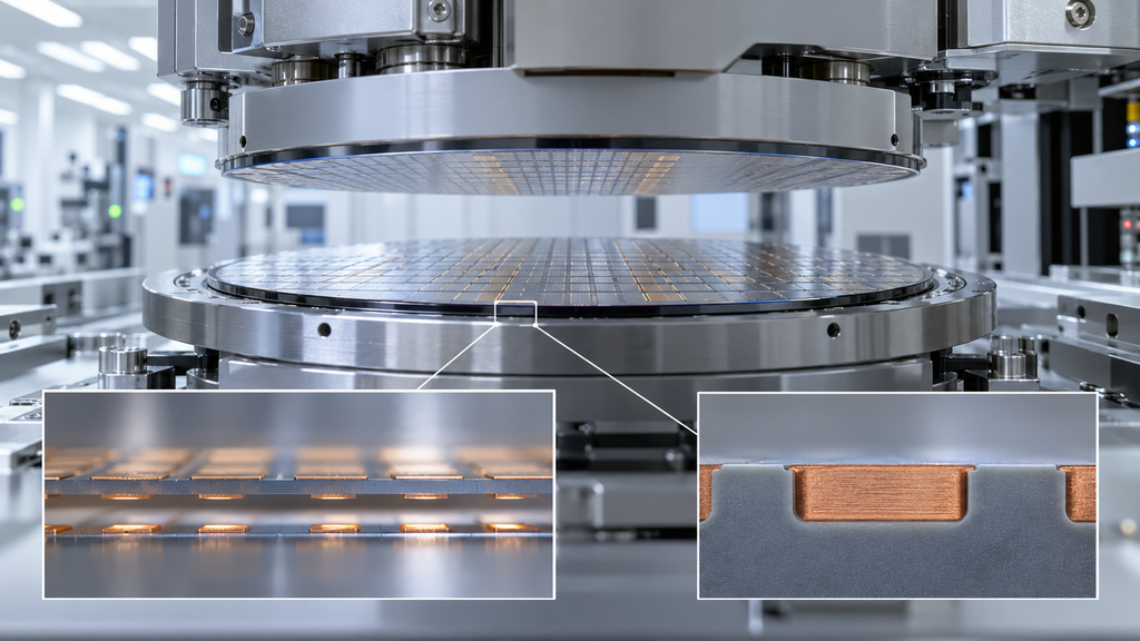
At 1.4 µm pitch, that process window becomes much smaller.
The key parameters increasingly become:
Wafer Flatness + Cu Recess + Surface Quality + Alignment + Particle Control
Sony Semiconductor Solutions is scheduled to present new results on October 20, 2026 at IMPACT-IAAC 2026 covering 1.4 µm-pitch Chip-on-Wafer hybrid bonding, including bonding misalignment behavior, Cu recess countermeasures and electrical characteristics.
This is a useful indication of where fine-pitch hybrid bonding is heading.
The challenge is no longer simply whether two copper pads can bond.
The challenge is whether millions of extremely small pads can bond simultaneously with sufficiently high yield.
What Is Hybrid Bonding?
Conventional semiconductor packaging commonly connects dies using solder bumps or microbumps.
A simplified structure looks like:
Chip
↓
Solder / Microbump
↓
Underfill
↓
Second Chip or Substrate
As interconnect pitch decreases, solder bumps become increasingly difficult to scale.
The bump diameter, spacing and solder volume eventually limit how closely connections can be placed.
Hybrid bonding removes much of this limitation.
Instead of relying on a solder bump, two extremely flat surfaces are bonded together.
The interface typically combines:
Cu-to-Cu electrical connection
with
dielectric-to-dielectric bonding
such as SiO₂-to-SiO₂.
A simplified structure becomes:
Dielectric + Cu Pad
↓
Direct Bond Interface
↑
Cu Pad + Dielectric
The result is a much shorter electrical path.
This enables:
- smaller pitch;
- higher I/O density;
- lower parasitic resistance and capacitance;
- improved bandwidth;
- better power efficiency;
- and thinner 3D structures.
These characteristics are particularly attractive for AI and memory systems, where enormous amounts of data need to move between vertically integrated semiconductor devices.
Why 1.4 µm Pitch Matters
A 1.4 µm interconnect pitch means the center-to-center spacing between neighboring electrical connections is approximately:
0.0014 mm
At this scale, an error of only a few hundred nanometers becomes a significant percentage of the entire pad dimension.
Sony’s research on face-to-back Chip-on-Wafer hybrid bonding has demonstrated 1.4 µm-pitch connections and investigated the effects of Cu recess, wafer warpage and bonding misalignment.
In one published study involving approximately two million 1.4 µm-pitch Cu-Cu connections, different wafer-warpage conditions produced different alignment performance. The higher-warpage process showed poorer alignment accuracy and resulted in open defects.
This demonstrates an important point:
As pitch decreases, wafer geometry becomes an electrical-yield parameter.
Wafer Bow and Warp are no longer only mechanical specifications.
They directly influence whether the copper pads actually meet.
1. Wafer Flatness Becomes Part of the Alignment Budget
Hybrid bonding requires two surfaces to approach one another with extremely high geometric accuracy.
If either surface is excessively curved, different regions may contact at different positions or under different mechanical conditions.
Important geometry parameters include:
- Bow;
- Warp;
- TTV;
- local flatness;
- local slope;
- die curvature;
- and thickness uniformity.
These parameters are related but should not be treated as identical.
TTV
Total Thickness Variation describes the difference between the thickest and thinnest points of a wafer or die.
Poor TTV can influence backside thinning, bonding-head contact and final die coplanarity.
Bow
Bow describes the overall curvature of the wafer’s median surface relative to a reference plane.
Warp
Warp describes the total difference between the highest and lowest points of the median surface.
Local Flatness
For fine-pitch hybrid bonding, local flatness can become even more important than global wafer geometry.
A wafer may appear acceptable when measured globally while still containing small local distortions near the bonding interface.
At micron-scale pitch, those small local deviations can affect alignment and bond-front propagation.
Why Warpage Can Cause Misalignment
It may seem that wafer warpage should only affect vertical contact.
In reality, warped wafers and dies can also create lateral displacement during bonding.
When a curved wafer or die is mechanically flattened against another surface, the material deforms.
This can slightly stretch or compress the bonding surface.
The resulting dimensional change can shift the copper pads relative to each other.
Sony has investigated this effect directly.
Its research found that wafer warpage influenced bonding alignment at 1.4 µm pitch, while separate Chip-on-Wafer studies showed that chip warpage, chip thickness and deformation during bond-wave propagation can contribute to scaling-related misalignment.
This means alignment accuracy cannot be solved only by improving the bonder.
The entire structure matters:
Incoming wafer geometry → thinning → film stress → die shape → handling → placement → bond-wave propagation
Fine-pitch bonding therefore becomes a system-level geometry problem.
2. Cu Recess Becomes Extremely Sensitive
One of the most important hybrid-bonding parameters is Cu recess.
After copper electroplating and CMP, the copper pad is usually not perfectly level with the surrounding dielectric.
Depending on the process, the copper surface may sit slightly below the dielectric.
This depth difference is called Cu recess.
A simplified cross-section looks like:
Dielectric surface
— — — — — — —
↓ Cu recess
Cu pad
The recess is intentional to some degree because direct dielectric contact must occur without excessive copper protrusion interfering with initial bonding.
However, the copper pads still need to connect electrically.
After initial dielectric bonding, thermal annealing allows copper to expand and form a stronger Cu-Cu connection.
The process window is therefore delicate.
If the Cu recess is too deep:
the pads may fail to contact.
If the copper protrudes too far:
the dielectric surfaces may not bond correctly.
Smaller Pads Make Cu Recess Harder to Control
This problem becomes increasingly difficult as pad dimensions shrink.
Sony’s 2026 conference abstract specifically notes that as Cu pad size decreases, the acceptable Cu recess window becomes tighter because smaller copper pads provide less thermal expansion during annealing.
In other words:
Smaller pad → less Cu expansion → tighter recess tolerance
This explains why CMP is becoming one of the most critical processes in hybrid bonding.
CMP must simultaneously control:
- copper height;
- dielectric height;
- Cu recess;
- Cu dishing;
- surface roughness;
- across-wafer uniformity;
- and local pattern-density effects.
That is far more demanding than simply producing a polished-looking wafer.
CMP Is Becoming a Hybrid-Bonding Process
Chemical Mechanical Polishing has traditionally been associated with front-end semiconductor planarization.
Hybrid bonding is bringing that same level of surface control into advanced packaging.
Sony previously reported an advanced CMP process designed specifically to improve Cu recess control.
For pad sizes of 1.4 µm and 1.0 µm, the optimized process produced approximately 99% and 95% Kelvin connection yield, respectively, compared with approximately 90% and 50% using its conventional process.
This is an important result.
It shows that as interconnect dimensions shrink, relatively small changes in surface preparation can produce large changes in electrical yield.
The bonding tool alone does not determine the outcome.
The result begins much earlier with:
Electroplating → CMP → Cleaning → Surface Activation → Metrology → Bonding
Cu Dishing Is Another Important Variable
Cu recess and Cu dishing are related but not identical.
Dishing occurs when CMP removes copper preferentially from the center of a pad or feature.
Instead of remaining perfectly flat, the copper surface becomes slightly concave.
Recent 2026 research published in IEEE Transactions on Semiconductor Manufacturing found that Cu pad dimensions and spacing significantly affect dishing behavior and subsequent hybrid-bond quality.
In that study, smaller 4 µm pads exhibited less dishing and achieved void-free bonding, while larger pad structures experienced progressively greater dishing and incomplete Cu bonding.
The implication is important:
pad geometry itself affects the CMP process window.
Therefore, interconnect design and wafer planarization cannot be optimized independently.
3. Alignment Tolerance Shrinks with Pitch
Consider two large copper pads.
If one pad is shifted slightly relative to the other, there may still be substantial overlapping area.
Now shrink both pads dramatically.
The same absolute placement error consumes a much larger percentage of the available overlap.
This is why fine-pitch hybrid bonding requires extremely accurate:
- wafer alignment;
- die placement;
- rotation control;
- magnification correction;
- scaling compensation;
- distortion correction;
- and thermal stability.
For a 1.4 µm pitch structure, hundreds of nanometers of error can already become significant.
At still smaller pitches, the allowable error moves toward tens of nanometers.
Research presented at the 2026 IEEE Hybrid Bonding Symposium is already addressing sub-150 nm pitch wafer-to-wafer hybrid bonding, with alignment reduction identified as a central challenge.
This illustrates how aggressive the roadmap has become.
Wafer-to-Wafer vs Die-to-Wafer Alignment
There is an important distinction between different hybrid-bonding architectures.
Wafer-to-Wafer — W2W
Two complete wafers are aligned and bonded.
Advantages include:
- highly parallel processing;
- potentially high throughput;
- simultaneous bonding of many devices.
But every die on one wafer is effectively paired with the corresponding die on the second wafer.
Yield matching can therefore become an issue.
Die-to-Wafer — D2W
Individual known-good dies can be selected and placed onto a wafer.
Advantages include:
- known-good-die selection;
- heterogeneous integration;
- different die sizes;
- logic-memory integration;
- chiplet architectures.
However, each die must be:
picked → aligned → placed → bonded
This introduces additional placement and throughput challenges.
Sony’s 1.4 µm development is particularly relevant because it addresses Chip-on-Wafer, where individual die geometry and placement accuracy become crucial.
4. Surface Roughness Must Approach the Atomic Scale
Hybrid bonding is fundamentally a surface-contact process.
Two surfaces cannot bond uniformly if their microscopic roughness prevents intimate contact.
For this reason, extremely low surface roughness is required.
At conventional packaging scales, a surface that looks perfectly smooth may be more than adequate.
For direct dielectric bonding, however, nanoscale topography matters.
Surface irregularities may prevent the bonding front from propagating uniformly.
That can create:
- voids;
- incomplete dielectric bonding;
- incomplete Cu contact;
- local stress;
- and reliability problems.
The 2026 IEEE Hybrid Bonding Symposium identified surface topography, via depth, dishing, roughness, chemistry and contamination as key parameters influencing bond uniformity and yield.
This is why AFM and other nanoscale metrology tools increasingly become relevant to advanced packaging.
5. One Particle Can Affect Many Connections
At 1.4 µm pitch, contamination becomes extremely serious.
A particle sitting between two bonding surfaces can prevent intimate contact around the particle.
Instead of causing only one failed interconnect, the resulting unbonded region may span multiple neighboring pads.
Important contamination sources include:
- CMP residue;
- airborne particles;
- organic contamination;
- metal particles;
- photoresist residue;
- handling contamination;
- and wafer-edge particles.
Hybrid bonding therefore requires very strict cleaning and environmental control.
Applied Materials explicitly described next-generation advanced packaging in October 2026 as requiring the same kinds of precision processing, metrology, inspection and particle-defect control traditionally associated with front-end wafer fabrication.
This is one of the most important transitions occurring in advanced packaging.
The distinction between:
front-end wafer fabrication
and
back-end packaging
is becoming less clear.
6. Surface Activation Is Critical Before Bonding
Before hybrid bonding, the dielectric and copper surfaces typically undergo cleaning and activation.
The objective is to produce surfaces capable of bonding at relatively low temperatures.
Depending on the process, this may involve:
- plasma activation;
- wet cleaning;
- oxide removal;
- surface functionalization;
- and controlled drying.
A poor activation process may reduce bond strength even when alignment is perfect.
The surfaces must remain extremely clean between activation and bonding.
This makes the queue time and handling environment important process variables.
Hybrid bonding therefore requires control of both:
surface chemistry
and
surface geometry.
7. Annealing Completes the Cu-Cu Connection
Hybrid bonding often occurs in two broad stages.
First, the dielectric surfaces establish contact.
Then thermal annealing strengthens the interface and helps form the Cu-Cu electrical connection.
Copper expands during thermal processing.
This expansion is one mechanism that allows recessed copper pads to make contact.
But as pad dimensions shrink, this mechanism becomes increasingly sensitive to geometry.
Research presented by imec at the 2026 IEEE Hybrid Bonding Symposium indicates that at sub-micron pitch, conventional elastic expansion becomes extremely small, and surface-diffusion-driven Cu bulge-out begins to play a more important role in establishing copper contact.
This suggests another important roadmap change:
The physics of hybrid bonding itself evolves as interconnect dimensions shrink.
Processes optimized for 10 µm pitch cannot simply be scaled proportionally to 1 µm or sub-micron pitch.
8. Alignment Is Not Only a Machine Specification
When evaluating a hybrid-bonding system, it is tempting to look only at a bonder’s advertised placement accuracy.
But final electrical alignment depends on much more.
A simplified alignment budget may include:
Bonder placement error
Wafer distortion
Die distortion
Warpage-induced scaling
Thermal expansion
Film stress
Bond-wave deformation
Metrology error
The final pad-to-pad offset is the combined result.
This is why a machine capable of extremely precise placement may still produce poor yield if incoming wafer geometry is uncontrolled.
For material and wafer suppliers, this creates new opportunities.
Specifications such as:
- TTV;
- Bow;
- Warp;
- local flatness;
- surface roughness;
- and backside thickness uniformity
become increasingly important to advanced packaging.
9. Thin Dies Make the Problem Harder
Advanced 3D integration increasingly uses thin silicon.
Thinning reduces the vertical distance between stacked devices.
It can also reduce TSV length and total package thickness.
But thin dies are more flexible.
That makes them more sensitive to:
- film stress;
- handling;
- vacuum pickup;
- bonding-head pressure;
- and thermal deformation.
Sony has reported that thinner chips can experience greater stretch during Chip-on-Wafer bonding, affecting scaling and alignment.
This creates a direct connection between:
wafer thinning quality
and
hybrid-bonding accuracy.
A wafer-thinning process therefore needs to control more than final thickness.
It should also manage:
- TTV;
- residual stress;
- backside damage;
- edge profile;
- die curvature;
- and post-thinning Warp.
10. Why 1.4 µm Is Particularly Relevant to AI and 3D Integration
Sony’s historical leadership in hybrid bonding has been strongly associated with CMOS image sensors.
However, the same fundamental technologies are highly relevant to broader 3D semiconductor integration.
AI processors increasingly require closer integration between:
- logic;
- cache;
- SRAM;
- HBM;
- accelerator chiplets;
- and specialized I/O dies.
Reducing interconnect pitch increases the number of electrical connections that can fit within a given area.
More connections can provide:
- higher bandwidth;
- shorter signal paths;
- lower energy per bit;
- improved power delivery;
- and greater 3D integration density.
This is why hybrid bonding is attracting growing attention beyond image sensors.
On October 1, 2026, Applied Materials and Besi expanded their hybrid-bonding collaboration specifically around next-generation 3D IC scaling, logic-memory integration, AI and photonics applications.
Their roadmap now includes new die-to-wafer platforms as well as die-on-wafer, die-on-die and die-on-panel integration.
11. 1.4 µm Is Not the Absolute Hybrid-Bonding Limit
This point is important when discussing the technology.
A headline such as:
“Hybrid bonding has reached 1.4 µm”
can be misleading.
Different bonding architectures have already demonstrated smaller pitches.
Sony previously reported 1 µm wafer-level face-to-face Cu-Cu hybrid bonding, while its publications also describe 0.4 µm-pitch wafer-to-wafer hybrid-bonding research.
The significance of the current 1.4 µm work is different.
It concerns the practical challenge of bringing extremely fine pitch into Chip-on-Wafer / face-to-back integration, where individual die placement, die warpage and alignment become much more complicated.
Therefore, the correct interpretation is:
Hybrid bonding overall is already moving below 1 µm in research, while 1.4 µm Chip-on-Wafer bonding represents an important step toward practical ultra-fine-pitch heterogeneous integration.
12. Key Parameters for Fine-Pitch Hybrid Bonding
For engineers evaluating wafers or dies for advanced bonding, several parameters should be considered together.
| Parameter | Why It Matters |
|---|---|
| TTV | Influences die thickness and coplanarity |
| Bow | Indicates overall wafer curvature |
| Warp | Influences alignment and bonding contact |
| Local Flatness | Controls local bond interface geometry |
| Surface Roughness | Affects direct dielectric bonding |
| Cu Recess | Determines whether Cu pads connect after annealing |
| Cu Dishing | Reduces effective Cu contact |
| Pad Pitch | Determines interconnect density |
| Pad Diameter | Affects overlap and Cu expansion |
| Alignment Accuracy | Determines pad-to-pad overlap |
| Particle Density | Strongly affects void formation |
| Surface Chemistry | Controls bond activation and strength |
| Die Thickness | Influences deformation and scaling |
| Residual Stress | Can change die/wafer geometry |
The important point is that these specifications are interconnected.
A wafer with excellent roughness but poor Warp may still create bonding problems.
Perfect alignment cannot compensate for excessively deep Cu recess.
Low TTV alone cannot compensate for particles.
Hybrid bonding therefore requires the complete interface to be treated as one integrated system.
From Micrometers to Nanometers
The evolution of hybrid bonding can be summarized as a transition in manufacturing precision.
Traditional packaging was largely governed by:
tens or hundreds of micrometers.
Fine-pitch microbumps moved the industry toward:
tens of micrometers.
Hybrid bonding pushes interconnection into:
single-digit micrometers, 1 µm and eventually sub-micron dimensions.
As this happens, the manufacturing priorities also change.
The industry increasingly moves from:
bump formation → surface engineering
placement → nanometer-scale alignment
package flatness → wafer-level planarization
visual inspection → nanoscale metrology
back-end cleanliness → front-end-level contamination control
This is why fine-pitch hybrid bonding should not be viewed simply as a new bonding technique.
It is part of a broader transformation in which advanced packaging increasingly inherits the precision requirements of semiconductor wafer fabrication.
Sony’s upcoming October 20, 2026 presentation on 1.4 µm Chip-on-Wafer hybrid bonding, together with current research on Cu recess, warpage and alignment, provides a clear example of this transition.
And the latest Applied Materials–Besi partnership demonstrates that the same technology is increasingly being positioned for AI, logic-memory integration and future 3D IC manufacturing.
For wafer suppliers, precision-processing companies and advanced-material manufacturers, that creates a clear technical message:
The future of advanced packaging will depend not only on smaller interconnects, but on tighter control of every surface and every micron of wafer geometry.