
The heartbeat of the semiconductor industry is maintained by highly sophisticated core equipment, each worth millions of dollars. Engineers monitor circuits thousands of times finer than human hair through precision windows, ensuring every step in modern chip manufacturing meets the highest standards. Every breakthrough in semiconductor technology relies directly on advances in these devices, which are positioned at the upstream of the industry chain. The global semiconductor manufacturing equipment market continues to expand in 2026, highlighting the strategic and economic significance of these machines.
1. Industry Landscape: Equipment Value and Distribution
A single state-of-the-art extreme ultraviolet (EUV) lithography machine can cost hundreds of millions of dollars and contains hundreds of thousands of components—far more complex than the core parts of an automobile. Semiconductor manufacturing resembles an ultra-precise relay race, where each process relies on specific equipment. Front-end wafer fabrication accounts for the majority of equipment investment, reflecting both the high technical barriers and uneven value distribution across device types.
Key categories of core equipment include:
| Equipment Type | Share of Front-End Value | Market Concentration | Domestic Status |
|---|---|---|---|
| Lithography | ~24% | Highly concentrated | Breakthrough stage in mature processes |
| Etching | ~20% | Highly concentrated | Rapid domestic progress |
| Thin Film Deposition | ~20% | Concentrated | Catching-up stage |
| Process Control & Inspection | ~11% | Leading global players | Early domestic breakthroughs |
| Wafer Cleaning | ~5% | Moderate | Partially localized |
| Chemical Mechanical Polishing (CMP) | ~4% | Moderate | High domestic penetration (>50%) |
| Ion Implantation | ~3% | High barrier | From 0 to 1 domestic achievement |
| Photoresist Coating & Development | <3% | Highly concentrated | Initial breakthroughs |
| Oxidation/Diffusion | ~2% | Concentrated | High domestic coverage in mature processes |
| Resist Stripping | Small share | Relatively dispersed | Near full domestic replacement |
2. Lithography: The Pinnacle of Technology
Lithography transfers circuit patterns onto silicon wafers, directly determining chip integration and performance limits. The process relies on precise optical projection systems and follows the Rayleigh criterion (CD = k₁·λ/NA) to push the boundaries of resolution. Globally, the market is oligopolistic. Achieving domestic capability for mature processes (≥90nm) remains a strategic priority, and ongoing efforts focus on further extending capabilities toward advanced nodes.
3. Etching: Precision in Three Dimensions
Etching removes specific materials from wafers beneath patterned masks to form intricate 3D structures. As chip designs transition from 2D to 3D architectures, the number and importance of etching steps increase. Dry etching, especially plasma-based etching, is the mainstream technology. Domestic equipment in this sector has achieved rapid progress, with advanced etchers capable of high aspect ratio processing suitable for 3D NAND manufacturing.
4. Thin Film Deposition: Building the Chip “Blocks”
Thin film deposition grows or coats layers of functional materials—conductors, insulators, or semiconductors—on the wafer surface, forming the essential “building blocks” of the chip. Key deposition techniques include Physical Vapor Deposition (PVD), Chemical Vapor Deposition (CVD), and Atomic Layer Deposition (ALD), with CVD being the most widely used. Domestic technology has made notable breakthroughs in PECVD, PVD, and MOCVD systems, covering multiple metallization and compound semiconductor applications.
5. Other Critical Equipment
Other essential devices support chip fabrication and ensure yield and quality:
- Process Control & Inspection: Monitors nanometer-scale fabrication steps to maintain yield. Technology barriers are high, but domestic systems are beginning to bridge the gap.
- Ion Implantation: Alters electrical properties of semiconductors. Domestic high-energy ion implanters have achieved “0 to 1” breakthroughs.
- Chemical Mechanical Polishing (CMP): Ensures global wafer planarization. Domestic CMP systems now exceed 50% market share for ≥28nm processes.
- Wafer Cleaning: Integral for defect-free fabrication. Domestic cleaning systems have reached a relatively high localization rate.
6. Industry Opportunities and Challenges in 2026
The rise of domestic semiconductor equipment is driven by a combination of technology, market demand, and policy support. Large-scale expansion of wafer fabrication facilities provides valuable testing grounds, while national funds accelerate innovation. Current breakthroughs focus on mature processes (≥28nm), with the aim to cover advanced nodes over time. Certain segments, such as lithography, high-end metrology, and ion implantation, remain difficult challenges. Semiconductor equipment is inherently capital, talent, and technology-intensive, requiring long-term development and ecosystem collaboration.
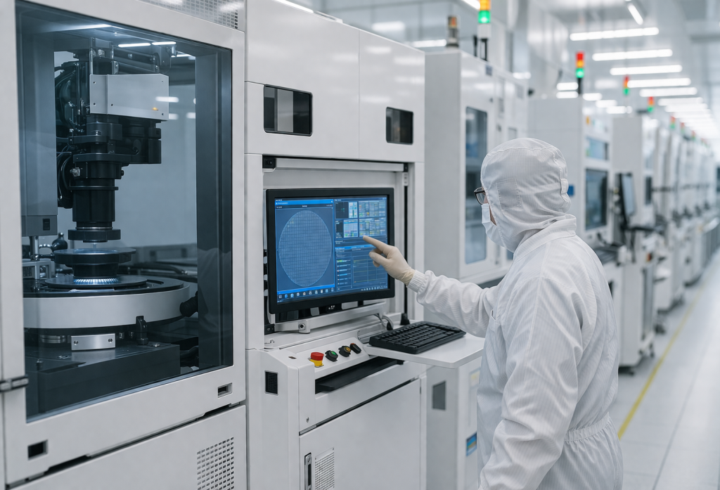
Inside a cleanroom, robotic arms steadily load wafers into domestic etching machines. Real-time nanometer-scale monitoring ensures stable parameters and target yields. Engineers record data—a testament to the successful validation of domestic equipment. Meanwhile, prototypes of next-generation lithography machines undergo careful calibration, their light sources glowing softly. A wall slogan reads: “Every nanometer of progress is measured by our own hand.”