
1. Introduction: Industry Context and Engineering Background
In advanced semiconductor packaging, the continuous demand for higher bandwidth, lower signal loss, and improved thermal stability is driving a transition from traditional organic substrates toward more advanced interconnect materials.
Based on observed industrial development trends in advanced packaging and substrate manufacturing lines, glass substrates have increasingly demonstrated strong potential in high-frequency and high-density applications due to their:
- Low dielectric constant (Dk)
- Low dielectric loss (Df)
- Độ ổn định cao về kích thước
- Excellent electrical insulation properties
Among glass-based interconnect technologies, Through Glass Via (TGV) has emerged as a key enabling solution for next-generation packaging architectures including 2.5D interposers, RF modules, and high-performance computing systems.
2. Technical Definition of TGV (Through Glass Via)
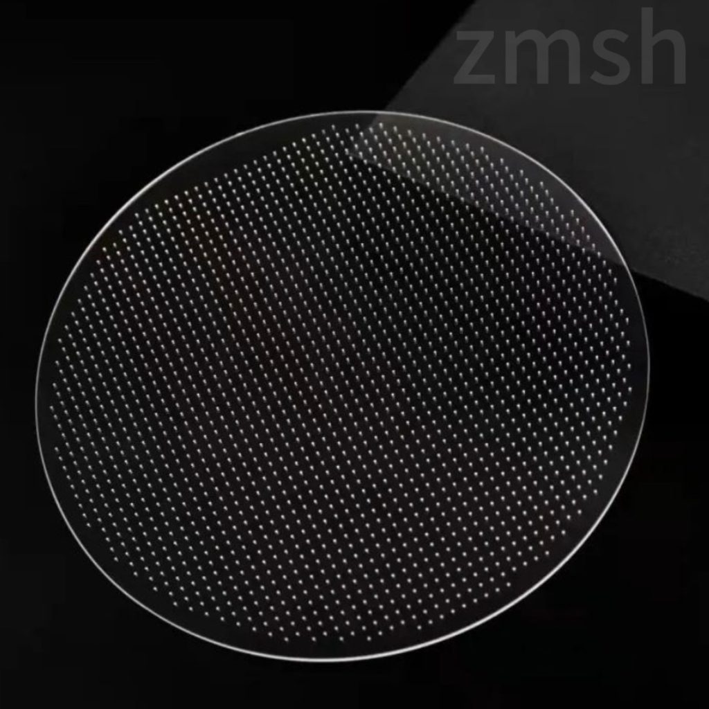
Through Glass Via (TGV) refers to a vertical interconnection structure formed by creating micro-scale vias in a glass substrate, followed by metallization to establish electrical connectivity between both surfaces.
From a manufacturing standpoint, TGV is not a single process, but a multi-stage integrated system combining laser modification, wet etching, metallization, electroplating, and planarization technologies.
Compared with silicon via technology (TSV), TGV provides:
- Lower RF signal attenuation
- Reduced parasitic capacitance
- Improved high-frequency transmission stability
- Enhanced dimensional control at wafer level
- Better optical-electrical integration compatibility
These characteristics make TGV particularly suitable for RF front-end modules, AI packaging interposers, and optoelectronic integration platforms.
3. Via Formation Engineering Capabilities (Process-Level View)
In industrial production environments, TGV via formation is typically achieved through a hybrid process of laser modification and chemical etching.
3.1 Structural Processing Capability
Current mature process capability ranges include:
- Aspect ratio up to 15:1
Supporting deep via formation in thin glass substrates. - Glass thickness range: 0.2 mm to 1.5 mm
Covering ultra-thin devices and standard interposer platforms. - High geometric precision control:
- Circularity > 95%
- Waist ratio > 0.9
These parameters indicate stable via morphology, which is critical for ensuring uniform metallization and minimizing electrical resistance variation.
3.2 Engineering Insight (Process Stability Consideration)
From a manufacturing perspective, maintaining via geometry consistency is one of the key determinants of yield. Inconsistent via profiles can lead to:
- Non-uniform seed layer deposition
- Voiding during electroplating
- Increased electrical resistance variation
Therefore, laser alignment accuracy and etching isotropy control are critical process parameters.
4. Metallization and Copper Filling Technology
TGV metallization is widely recognized as one of the most technically challenging steps due to the high aspect ratio and confined geometry of glass vias.
4.1 Multi-Layer Copper Deposition Process
A typical industrial process flow includes:
- Sputtering (seed layer formation)
- Electroless copper deposition
- Electroplating (via filling)
- Đánh bóng hóa học cơ học (CMP)
This multi-stage approach ensures:
- Continuous conductive pathways
- Uniform copper distribution along via sidewalls
- Stable electrical performance across wafer-level structures
4.2 Process Engineering Challenges
Based on industrial process characteristics, key technical challenges include:
- Mass transport limitation in high aspect ratio vias
- Ion distribution uniformity during electroplating
- Stress accumulation during copper deposition
- Interface adhesion reliability between glass and metal layers
Advanced plating system design and flow field optimization are typically required to mitigate these effects.
5. Equipment System Architecture and Process Integration
In industrial TGV manufacturing lines, equipment performance directly determines process yield, especially in wet process environments.
5.1 Via Drying and Defect Control System
After wet processing steps, via drying systems are used to:
- Reduce liquid residue-induced micro-cracking
- Improve structural stability of etched vias
- Increase overall yield in post-etch processes
5.2 Copper Process and Mechanical Reliability Optimization
Copper-related process equipment contributes to:
- Reduction of mechanical breakage during polishing
- Improved adhesion strength between layers
- Enhanced via reliability under thermal cycling
5.3 Laser Modification Precision Control
Laser systems used in TGV formation provide:
- Stable modification paths in brittle glass materials
- High perpendicularity of via sidewalls
- Accurate positional alignment across large-area substrates
These factors significantly impact downstream etching uniformity and metallization success rate.
6. Integrated TGV Manufacturing Process Flow
A typical industrial TGV production system can be divided into three major modules:
6.1 Via Formation Module
Process sequence:
Laser modification → Wet etching → AOI inspection
Material transformation:
Glass substrate → High-precision glass via structure
Thiết bị chính:
- Glass via etching system (Wet Bench)
6.2 Metallization & Filling Module
Process sequence:
Sputtering → Electroless plating → Electroplating → CMP
Thiết bị chính:
- Pre-clean wet bench system
- Electroless copper plating system
- Double-side electroplating system (rack plating configuration)
This module determines electrical conductivity and long-term reliability.
6.3 Redistribution Layer (RDL) Formation Module
Process sequence:
Photoresist coating → Lithography → Development → Etching
Thiết bị chính:
- Development wet bench system
- UBM etching system (single-wafer glass processing)
This stage enables lateral interconnect routing for chip-level integration.
7. Reliability and Manufacturing Challenges
Despite its advantages, TGV technology still faces several engineering and industrialization challenges:
- High aspect ratio copper void control
- Thermal stress management in brittle glass materials
- Micro-crack suppression during wet/dry transitions
- Cross-contamination control in wet bench environments
- Large-area substrate uniformity control
From an industrial yield perspective, these challenges are primarily addressed through equipment-level optimization and process integration rather than single-step improvements.
8. Industry Development Trends and Future Outlook
Based on current semiconductor packaging development trajectories, TGV technology is expected to evolve toward:
- Aspect ratios exceeding 20:1
- Fully automated wet process integration platforms
- Low-stress copper filling materials and barrier systems
- High-frequency (RF/mmWave) optimized interposer structures
- AI computing and HPC packaging integration
With the rapid expansion of AI-driven computing infrastructure, TGV is expected to become a key enabling technology in next-generation advanced packaging ecosystems.
9. Conclusion
Công nghệ Through Glass Via (TGV) represents a critical advancement in semiconductor interconnect engineering, transforming glass substrates from passive insulating materials into functional high-density interconnection platforms.
Its key technical advantages include:
- High-density vertical interconnect capability
- Excellent RF and electrical performance
- Superior dimensional stability
- Strong compatibility with advanced packaging architectures
From an industrial perspective, the success of TGV implementation relies heavily on the integration of laser processing systems, wet etching equipment, and advanced electroplating platforms.
As advanced packaging continues to evolve toward higher performance and lower signal loss requirements, TGV is expected to play an increasingly important role in AI, RF, and optoelectronic integration systems.