
Поскольку стеклянные подложки приобретают всё большее значение в сфере передовых технологий упаковки полупроводников, прецизионные отверстия, изготовленные в стеклянных пластинках, играют ключевую роль в создании электронных устройств нового поколения. Эти отверстия служат каналами для электрических соединений, прохождения жидкостей, передачи света, выравнивающих структур и специальных элементов упаковки.
В отличие от традиционной обработки кремния, создание отверстий в стеклянных пластинках сопряжено с особыми сложностями, поскольку стекло является хрупким материалом, который очень подвержен сколам по краям, образованию микротрещин и возникновению остаточных напряжений. Для получения чистых отверстий с точными размерами требуется тщательный подбор методов обработки, технологических параметров и методов контроля.
В данной статье рассматриваются процесс вырезания отверстий в стеклянных подложках, существующие технологии производства, типичные проблемы, связанные с качеством, а также основные аспекты проектирования для применения в полупроводниковой промышленности и сфере передовых технологий упаковки.
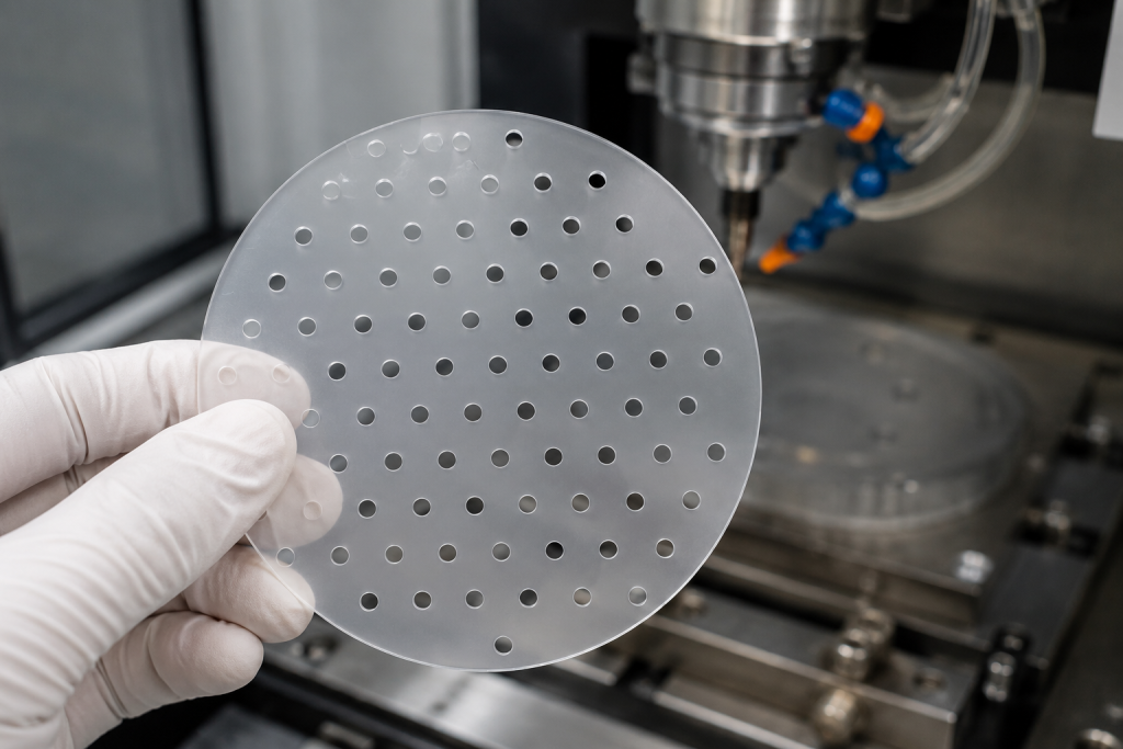
Что такое вырезание отверстий в стеклянных пластинках?
Вырезание отверстий в стеклянных пластинках — это процесс создания прецизионных круглых отверстий или полостей в стеклянной пластинке с сохранением структурной целостности окружающего материала.
Полученные отверстия можно использовать для:
- Подготовка сквозных переходов через стекло (TGV)
- Интеграция датчиков
- Оптические тракты
- МЭМС-устройства
- Микрожидкостные системы
- Упаковка на уровне пластин
- Центровальные отверстия
- Механическое позиционирование
- Вакуумная упаковка
- Конструкции полупроводниковых промежуточных слоев
В зависимости от области применения отверстие может быть:
- Полное сквозное отверстие
- Слепое отверстие
- Углубление
- Ступенчатое отверстие
- Прецизионное зенкерование
Требуемая геометрия определяет подходящий технологический процесс.
Почему стекло используется в современных упаковочных решениях
Стекло стало привлекательным материалом-подложкой благодаря сочетанию превосходных электрических, механических и тепловых свойств.
По сравнению с органическими подложками стекло обладает следующими преимуществами:
- Превосходная стабильность размеров
- Низкие диэлектрические потери
- Высокая электрическая изоляция
- Гладкая поверхность
- Незначительные колебания коэффициента теплового расширения
- Высокая плоскостность
- Хорошая оптическая прозрачность
- Совместимость со слоями перераспределения с мелким шагом
По сравнению с кремнием стекло, как правило, обеспечивает меньшие потери радиочастотного сигнала и более высокую эффективность в высокочастотных системах.
По мере дальнейшего развития архитектур на основе чиплетов, процессоров искусственного интеллекта и гетерогенной интеграции стеклянные промежуточные слои привлекают всё большее внимание производителей полупроводников.
Почему бурение с извлечением керна сложнее, чем кажется
Хотя стекло кажется относительно мягким по сравнению с сапфиром или карбидом кремния, при механической обработке оно ведет себя как хрупкий материал.
В отличие от пластичных металлов стекло при нагрузке скорее разрушается, чем подвергается пластической деформации.
В ходе отбора проб ненадлежащий контроль технологического процесса может привести к:
- Скол края
- Радиальные трещины
- Подземные повреждения
- Остаточное напряжение
- Царапины на поверхности
- Конические отверстия
- Загрязнение частицами
- Угловые переломы
Эти дефекты могут снизить выход готовой продукции и повлиять на последующие этапы производства, такие как металлизация, формирование TGV и склеивание пластин.
Распространенные технологии вырезания отверстий в стеклянных пластинках
В зависимости от размера отверстия, толщины пластины, требований к допускам и объема производства можно использовать несколько методов изготовления.
Механическое колонковое бурение
Бурение алмазным коронным сверлом является одним из традиционных способов создания относительно больших отверстий.
Преимущества включают:
- Отлаженная технология
- Хороший контроль размеров
- Подходит для изготовления прототипов
- Совместим с различными типами стекла
Однако механический контакт приводит к возникновению режущих сил, которые могут повысить риск образования сколов и микротрещин.
Крайне важно обеспечить правильную подачу охлаждающей жидкости, скорость вращения шпинделя и скорость подачи.
Ультразвуковая обработка
Ультразвуковая обработка сочетает в себе высокочастотные колебания и абразивную суспензию для удаления хрупких материалов.
К преимуществам относятся:
- Меньшие усилия резания
- Снижение повреждений кромок
- Повышенная прочность для хрупкого стекла
- Подходит для точных прорезов
Ультразвуковая обработка часто выбирается в тех случаях, когда необходимо свести к минимуму механические нагрузки.
Лазерное сверление
Лазерное сверление отверстий становится всё более популярным в полупроводниковой промышленности.
Вместо механической резки сфокусированная лазерная энергия изменяет или удаляет материал без физического контакта с режущим инструментом.
Преимущества включают:
- Возможность обработки мелких отверстий
- Высокая точность позиционирования
- Гибкая геометрия
- Снижение механической нагрузки
- Отличный потенциал автоматизации
Сверхбыстрые лазерные системы позволяют ещё больше уменьшить зоны термического влияния и количество микротрещин.
Лазерное сверление отверстий особенно подходит для современных технологий монтажа и прецизионной микроэлектроники.
Обработка с использованием струи воды
Для обработки некоторых проемов больших размеров может применяться абразивная гидроабразивная резка.
Несмотря на то что этот метод оказывает относительно небольшое термическое воздействие, без дополнительных процессов финишной обработки он, как правило, не позволяет достичь той же точности размеров, которая требуется при производстве полупроводниковых корпусов.
Гибридное производство
Многие производители сочетают несколько технологий в рамках одной производственной линии.
Например:
- Предварительное лазерное сверление
- Механическая обработка
- Полировка кромок
- Очистка
- Контроль поверхности
Гибридная обработка позволяет повысить как производительность, так и качество конечной продукции.
Рекомендации по проектированию проемов для прецизионного стекла
Успешное вырезание отверстий в стеклянных пластинках начинается с правильного проектирования изделия.
Диаметр отверстия
Чем меньше отверстия, тем, как правило, строже должен быть контроль производственного процесса.
Размер отверстия влияет на:
- Метод механической обработки
- Время цикла
- Соотношение сторон
- Качество кромок
- Сложность проверки
- Себестоимость производства
По возможности конструкторам следует избегать использования неоправданно малых диаметров.
Толщина пластины
Взаимосвязь между толщиной пластины и диаметром отверстия напрямую влияет на сложность обработки.
Большое соотношение сторон затрудняет:
- Уборка мусора
- Качество боковых стенок
- Точность размеров
- Прямолинейность отверстия
Более тонкие пластины позволяют уменьшить глубину сверления, но требуют дополнительных мер по обеспечению безопасности при обращении с ними.
Положение отверстия
Точность позиционирования особенно важна для:
- Массивы TGV
- Оптическая центровка
- Многочиповая упаковка
- Структуры МЭМС
- Интеграция датчиков
Опорные точки должны быть чётко обозначены на технических чертежах.
Расстояние до края
Недостаточное расстояние между отверстием и краем пластины повышает риск поломки.
Инженеры должны оставлять вокруг каждого отверстия достаточный запас материала для обеспечения механической прочности на протяжении всего процесса обработки.
Качество поверхности и боковых стенок
Качество отверстия оценивается по ряду характеристик.
Цикличность
Готовое отверстие должно максимально соответствовать задуманной круглой форме.
Недостаточная круглость может затруднить нанесение металлического покрытия и сборку компонентов.
Цилиндричность
В случае сквозных отверстий стенки должны оставаться максимально прямыми.
Чрезмерное сужение может негативно повлиять на процесс нанесения покрытия TGV и электрические характеристики.
Шероховатость боковых стенок
Гладкие боковые стенки улучшают:
- Нанесение металла
- Адгезия
- Электротехническая надежность
- Течение жидкости
- Оптические характеристики
Для сложных задач может потребоваться дополнительная полировка.
Сколы по краям
Небольшие сколы вокруг входа или выхода из отверстия могут стать местами зарождения трещин.
Поэтому перед последующей обработкой качество кромок тщательно проверяется.
Очистка после бурения
В процессе механической обработки образуются частицы, абразивные остатки и микроскопические осколки стекла.
Уборка, как правило, включает в себя:
- Промывка деионизированной водой
- Ультразвуковая очистка
- Химическая чистка
- Удаление частиц
- Сушка
- Контроль поверхности
Чистота имеет особое значение перед металлизацией или склеиванием пластин.
Методы проверки
Контроль отверстий в стеклянных пластинках обычно осуществляется с помощью нескольких методов метрологии.
Оптическая микроскопия
Используется для:
- Чипы Edge
- Дефекты поверхности
- Обнаружение трещин
- Геометрия отверстия
Системы координатно-измерительных приборов
Размер:
- Диаметр отверстия
- Точность позиционирования
- Расстояние между отверстиями
- Цикличность
3D-оптическая профилометрия
Содержит информацию по следующим вопросам:
- Шероховатость поверхности
- Высота ступени
- Профиль кромки
- Геометрия боковых стенок
Автоматический визуальный контроль
В производственных условиях для контроля качества при массовом производстве часто используются автоматизированные системы контроля.
Эти системы повышают стабильность качества и сокращают время проведения проверок.
Типичные проблемы в сфере производства
Микротрещины
Микротрещины могут быть незаметны при первоначальном осмотре, но могут распространяться в ходе термоциклирования или при манипуляциях с пластинками.
Оптимизированные параметры обработки помогают свести к минимуму их образование.
Генерация частиц
Стеклянные частицы могут привести к загрязнению последующих этапов производства полупроводников.
Надлежащий расход охлаждающей жидкости, процедуры очистки и техническое обслуживание оборудования позволяют снизить уровень загрязнения.
Коничность отверстия
Износ инструмента или неправильные настройки технологического процесса могут привести к образованию конических отверстий.
Для применения в технологии TGV геометрия боковых стенок имеет особое значение, поскольку она влияет на последующую металлизацию.
Остаточные напряжения
Механическая или термическая обработка может привести к возникновению внутренних напряжений.
Стресс может привести к появлению отложенных трещин во время упаковки или испытаний на надежность.
Области применения технологии вырезания отверстий в стеклянных пластинках
В современном производстве полупроводников широко используются прецизионные стеклянные отверстия.
К типичным областям применения относятся:
Проходная перемычка через стекло (TGV)
При сверлении отверстий в стекле создаются исходные отверстия, которые впоследствии металлизируются для формирования электрических соединений.
Устройства MEMS
Многие датчики MEMS требуют наличия точно расположенных полостей и каналов для прохождения жидкости.
Оптическая упаковка
Стеклянные отверстия позволяют интегрировать оптические волокна, линзы и фотонные компоненты в компактные корпуса.
Биомедицинские микросхемы
Микрожидкостные устройства часто основаны на стеклянных каналах и резервуарах, изготовленных с высокой точностью.
Упаковка RF
Стеклянные подложки обеспечивают работу высокочастотных устройств связи с превосходной целостностью сигнала.
Упаковка на уровне пластин
Благодаря высокоточным отверстиям становится возможной компактная интеграция нескольких функциональных слоев в современных полупроводниковых корпусах.
Информация, необходимая для изготовления на заказ
При запросе коммерческого предложения на вырезание отверстий в стеклянных пластинках покупатели должны предоставить:
- Стекло
- Диаметр пластины
- Толщина пластины
- Диаметр отверстия
- Глубина отверстия
- Количество вакансий
- Допуск по положению
- Качество поверхности
- Требования к боковым стенкам
- Качество кромок
- Файл чертежа
- Объем производства
- Требования к проверке
Подробные чертежи помогают производителям подобрать наиболее подходящий технологический процесс.
Часто задаваемые вопросы
В чём заключается разница между вырезанием отверстий в стеклянных пластинках и их сверлением?
Под термином «коринг» обычно понимается создание прецизионных отверстий с контролируемой геометрией и минимальным повреждением, тогда как «сверление» — это более общий термин в области механической обработки. При производстве полупроводников часто требуются гораздо более жесткие допуски, чем при обычном сверлении.
Может ли лазерное вырезание ядра устранить сколы по краям?
Лазерная обработка позволяет значительно снизить механические повреждения, однако при неправильном выборе параметров процесса все же могут возникать термические дефекты или микротрещины.
Какой процесс лучше всего подходит для производства TGV?
Выбор оптимального метода зависит от размера отверстия, толщины пластины, соотношения сторон, объема производства и требований к металлизации. Многие производители сочетают лазерную обработку с последующими этапами финишной обработки.
Можно ли изготовить очень мелкие отверстия в стеклянных пластинках?
Да. Сверхбыстрые лазерные системы и специализированные технологии микрообработки позволяют создавать чрезвычайно малые отверстия с высокой точностью позиционирования.
Как проводится контроль качества отверстий?
Производители, как правило, оценивают диаметр, положение, конусность, качество боковых стенок, дефекты поверхности, сколы по краям и загрязнение частицами с помощью оптического и автоматизированного измерительного оборудования.
Влияет ли тип стекла на процесс вырезания отверстий?
Да. Боросиликатное стекло, плавленый кремнезем, кварцевое стекло и специальное упаковочное стекло обладают разными тепловыми и механическими характеристиками, что требует использования различных параметров обработки.
Заключение
Вырезание отверстий в стеклянных пластинках — это ключевой производственный процесс, обеспечивающий быстрый рост в таких областях, как передовые технологии упаковки полупроводников, МЭМС-устройства, фотоника и технология сквозных стеклянных переходов.
Для изготовления высококачественных отверстий требуется гораздо больше, чем просто просверлить отверстие. Выбор технологического процесса, параметры обработки, качество стенок отверстия, чистота и контроль качества — все эти факторы влияют на конечную надежность устройства.
По мере того как в области монтажа полупроводников продолжается переход к более мелким шагам и использованию стеклянных подложек больших размеров, прецизионное вырезание отверстий в стеклянных пластинках останется одной из ключевых технологий, обеспечивающих развитие электронных систем будущего.