
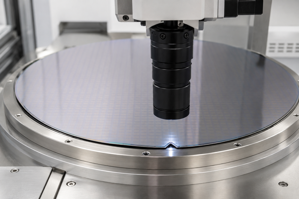
The notch on a 300 mm wafer is a small feature, but it performs several critical functions throughout semiconductor manufacturing. It provides a mechanical reference for wafer orientation, supports automated handling and helps equipment establish a repeatable coordinate system.
An incorrect or damaged notch can cause wafer-loading errors, pattern misalignment, incorrect dicing orientation and handling failures. These risks become especially important when processing patterned wafers, bonded wafers, expensive compound-semiconductor substrates or wafers requiring precise crystallographic alignment.
This guide explains common 300 mm wafer notch dimensions, orientation requirements, measurement methods and the role of the notch in wafer dicing alignment.
What Is a Wafer Notch?
A wafer notch is a V-shaped identification feature machined into the outer edge of a circular wafer.
The notch can be used to identify or establish:
- Wafer rotational orientation
- Crystal-axis orientation
- Front-side and back-side handling conventions
- Equipment loading position
- Wafer-map coordinates
- Lithography alignment
- Inspection coordinates
- Dicing-street direction
- Die row and column orientation
Older and smaller wafers may use one or more orientation flats. Large wafers typically use a notch because it removes less usable wafer area and is easier for automated equipment to detect.
The notch should not be treated as a general-purpose precision alignment mark. It provides an initial mechanical orientation reference, while high-accuracy processing normally relies on optical alignment marks or patterned wafer features.
Applicable Standards for 300mm Wafers
For 300 mm monocrystalline silicon wafers, the most commonly referenced dimensional standard is SEMI M1.
SEMI M1 covers the dimensional and selected material characteristics of polished single-crystal silicon wafers. The standard includes classifications for 300 mm polished silicon wafers with a notch and defined edge profiles. SEMI M1 standard description
However, the term “300 mm wafer” may also describe:
- Silicon test wafers
- SOI wafers
- Silicon carbide wafers
- Glass wafers
- Sapphire wafers
- Quartz wafers
- Ceramic carrier wafers
- Bonded wafers
- Reclaimed wafers
- Equipment qualification wafers
These materials should not automatically be assumed to have the same notch orientation or edge profile as a standard silicon wafer.
The purchase specification should always identify the material, crystallographic orientation, notch standard and applicable standard revision.
Common 300mm Silicon Wafer Notch Dimensions
The following values are widely associated with notched 300 mm silicon wafers manufactured to conventional SEMI M1-type geometry.
| Параметр | Common specification |
|---|---|
| Диаметр пластины | 300.00 mm |
| Nominal notch depth | 1.00 mm |
| Notch-depth tolerance | +0.25/−0.00 mm |
| Nominal included angle | 90° |
| Notch-angle tolerance | +5°/−1° |
| Number of notches | One |
| Secondary fiducial | Normally none |
| Typical notch-axis orientation for standard silicon | Related to the specified crystallographic axis |
These values should be treated as a purchasing reference, not a replacement for the current controlled standard or customer drawing.
Standard revisions can change dimensional requirements. For example, SEMI documentation has recorded activities related to changing 300 mm wafer diameter tolerances. The standard revision and customer specification should therefore be listed explicitly on the purchase order.
Understanding the Main Notch Dimensions
Notch depth
Notch depth is the radial distance from the nominal wafer circumference to the deepest point of the notch.
It should not be confused with the distance from the actual local edge to an irregular or chipped notch apex.
A notch that is too shallow may be difficult for an equipment sensor to detect. A notch that is too deep removes additional edge material and may increase local stress concentration.
Notch angle
The notch angle is the included angle between the two notch sidewalls.
The angle influences:
- Sensor recognition
- Notch-center calculation
- Equipment compatibility
- Contact behavior in wafer-handling systems
- Local mechanical strength
- Repeatability of rotational alignment
The notch sides should form a controlled and symmetrical V shape. An asymmetric notch may shift the calculated notch center even if its maximum depth appears acceptable.
Notch-axis position
The notch axis is normally represented by a line extending from the wafer center through the geometrical center or deepest point of the notch.
This axis establishes the angular reference used by wafer-handling and processing equipment.
The notch-axis tolerance describes the allowed angular deviation between the actual notch axis and the specified crystallographic or mechanical reference axis.
Notch-tip radius and edge blending
The notch apex should not contain an uncontrolled sharp crack. A suitable tip condition and smooth edge transition help reduce mechanical stress and particle generation.
When a notch-tip radius is critical, it should be stated separately on the drawing. The included angle and depth alone do not fully describe the notch geometry.
Notch-edge profile
The notch edge may require:
- Шлифование
- Fine grinding
- Полировка
- Chemical finishing
- Controlled beveling
- Edge-damage removal
- Specific roughness limits
The required finish depends on whether the wafer is a prime substrate, dummy wafer, carrier wafer or custom mechanical part.
How the Notch Relates to Crystal Orientation
For a monocrystalline wafer, the surface orientation and notch orientation describe different directions.
For example, a silicon wafer may have a nominal surface orientation of (100), while the notch axis is aligned with an in-plane crystallographic direction such as ⟨110⟩.
The surface orientation describes the crystal plane parallel to the wafer surface. The notch orientation identifies an in-plane direction used as a rotational reference.
These two specifications should therefore be listed independently:
- Surface orientation
- Off-axis angle, if applicable
- Off-axis direction
- Notch-axis orientation
- Notch-axis tolerance
Silicon wafers
A conventional notched 300 mm (100) silicon wafer commonly uses the notch as a reference to an in-plane ⟨110⟩ direction. The exact requirement should be confirmed against the applicable SEMI M1 classification and revision.
Silicon carbide wafers
SiC uses different crystallographic notation and may also require a deliberate off-axis orientation for epitaxial growth.
A 300 mm 4H-SiC specification may separately define:
- Surface plane
- Off-axis angle
- Off-axis direction
- Notch orientation
- Notch angular tolerance
Published commercial SiC specifications demonstrate that a 300 mm SiC wafer can use a nominal notch depth of 1.0 mm and a nominal angle of 90°, while its crystallographic notch direction and tolerance are defined according to the SiC crystal system. Example 300 mm SiC specification
Therefore, a silicon notch-orientation requirement should never be copied directly into a SiC RFQ without verification.
Glass, quartz and ceramic wafers
Amorphous glass and fused quartz do not have a crystallographic orientation equivalent to single-crystal silicon.
For these materials, the notch normally serves as a mechanical reference. Its orientation may be related to:
- Pattern layout
- Dicing direction
- Coating orientation
- Laser marking
- Customer-defined zero position
- Equipment compatibility
For amorphous materials, the drawing should define the notch relative to an identifiable feature rather than referring to a nonexistent crystal axis.
Sapphire wafers
Sapphire is crystalline and anisotropic. Its surface plane, in-plane direction and notch orientation must be defined using the correct crystallographic convention.
A generic silicon-wafer notch callout is insufficient for a sapphire wafer.
Why Notch Orientation Matters in Wafer Dicing
Dicing equipment must understand how the die pattern is positioned relative to the wafer.
The notch may provide the first rotational reference when the wafer is loaded. The dicing system then uses cameras and alignment algorithms to locate streets, fiducials or die features.
A typical alignment sequence is:
- Load the wafer onto the dicing chuck.
- Detect the wafer edge.
- Locate the notch.
- Establish an approximate wafer center and rotational zero.
- Move to an optical alignment location.
- Detect streets or alignment marks.
- Correct X, Y and theta position.
- Confirm cutting direction.
- Begin the approved dicing sequence.
The notch is therefore an important coarse-alignment feature, but optical pattern alignment normally determines the final cut position.
Rotational Error and Linear Dicing Offset
A small angular error can create a large positional shift near the wafer edge.
The approximate lateral displacement is:
[
\Delta x \approx r\theta
]
where:
- (\Delta x) is the lateral displacement
- (r) is the distance from the wafer center
- (\theta) is the angular error in radians
For a feature located approximately 150 mm from the center of a 300 mm wafer, an angular error of 0.1° produces a lateral displacement of approximately:
[
150 \times \frac{0.1\pi}{180} \approx 0.262\ \text{mm}
]
A displacement of approximately 262 µm is much larger than many semiconductor dicing streets.
This example shows why notch-only alignment is generally insufficient for precision dicing. The equipment should perform optical theta correction using the actual wafer pattern.
Notch Position Versus Dicing-Street Direction
The notch-to-street relationship should be clearly documented.
Possible requirements include:
- Primary dicing streets parallel to the notch axis
- Primary streets perpendicular to the notch axis
- Die rows rotated by a defined angle from the notch
- Custom pattern orientation based on mask coordinates
- Different street directions on the front and back sides
- Alignment based on fiducials rather than notch geometry
A dicing map should identify:
- Wafer center
- Notch position
- X-axis direction
- Y-axis direction
- First cut direction
- Die numbering convention
- Active surface
- Viewing direction
- Exclusion zones
- Partial-die handling near the edge
Without these definitions, one party may view the wafer from the front while another interprets the map from the back. This can mirror the die layout and reverse the dicing sequence.
How to Define the Wafer Coordinate System
A practical wafer-coordinate system should specify:
- The active surface viewed from above
- Wafer center as the origin
- Notch direction
- Positive X direction
- Positive Y direction
- Clockwise or counterclockwise angular convention
- Zero-degree position
- Die row and column numbering
- Orientation of text or wafer ID marking
A common drawing convention places the notch at the bottom of the page. However, this graphical convention should not be assumed unless it is stated.
The drawing should include a note such as:
View from the polished front surface, with the notch at the 6 o’clock position.
If the wafer is double-side polished or contains patterns on both sides, the front-side definition must be especially clear.
How Wafer Notches Are Measured
Notch inspection can be performed using optical or dimensional measurement equipment.
Vision measurement system
A calibrated vision system captures the wafer edge and calculates:
- Wafer center
- Notch apex
- Notch depth
- Included angle
- Sidewall symmetry
- Notch-axis direction
- Edge defects
This is commonly suitable for automated inspection.
Optical comparator
An optical comparator can magnify the notch profile and compare it with a reference geometry.
It may be used to inspect:
- Depth
- Angle
- Tip condition
- Sidewall profile
- Чипы Edge
Coordinate measuring system
A suitable noncontact coordinate measurement system can collect multiple points along the wafer perimeter and notch.
The analysis software can fit the circular edge, determine the wafer center and calculate notch geometry relative to that fitted center.
Contact probes should be used carefully because thin or brittle wafers may be scratched, chipped or displaced.
Microscope inspection
A microscope is appropriate for evaluating:
- Microchips
- Следы шлифовки
- Cracks
- Residue
- Polishing condition
- Edge contamination
- Local surface defects
A microscope alone may not provide sufficient accuracy for determining notch-axis orientation unless it is integrated with a calibrated stage and measurement system.
Recommended Measurement Procedure
A controlled notch-measurement procedure may include the following steps:
- Clean the wafer using an approved method.
- Place it on a clean, flat, non-damaging support.
- Detect or measure the outer wafer edge.
- Fit the measured edge points to determine the wafer center.
- Exclude the notch region from the circle-fit calculation.
- Detect both notch sidewalls.
- Calculate the sidewall intersection or defined notch center.
- Measure radial notch depth.
- Calculate the included angle.
- Determine the notch axis relative to the wafer center.
- Inspect the tip and sidewalls for damage.
- Record the measurement method and uncertainty.
- Save the inspection image when traceability is required.
The method should define how the notch apex is calculated when the tip has a finite radius.
Common Notch Defects
Скол края
Small chips may form during grinding, polishing, handling or repeated equipment loading.
Chips can:
- Change optical detection
- Generate particles
- Reduce edge strength
- Produce an inaccurate notch center
Asymmetric sidewalls
If one notch side is longer or steeper than the other, the apparent notch axis may shift.
Excessive notch depth
A deep notch may reduce the usable edge area and increase local mechanical stress.
Insufficient notch depth
A shallow notch may not be detected reliably by equipment configured for standard geometry.
Rounded or damaged apex
A controlled tip radius is acceptable when specified. An irregular rounded region caused by chipping or wear is not equivalent to a controlled notch profile.
Surface contamination
Tape residue, particles or coatings inside the notch can interfere with edge sensors and optical inspection.
Incorrect angular orientation
The notch geometry may meet its dimensional limits but still be rotated incorrectly relative to the crystal direction or pattern.
Notch Requirements for Custom and Resized Wafers
Wafer resizing can create a smaller wafer from a larger substrate or produce a custom diameter. A new notch may then be required.
The customer should specify:
- Final wafer diameter
- Original wafer orientation
- Required final notch direction
- Notch geometry
- Notch-to-pattern relationship
- Ориентация кристаллов
- Front-side viewing direction
- Профиль кромки
- Surface finish inside the notch
- Allowed edge exclusion
- Angular tolerance
- Inspection method
The original wafer notch may be removed during resizing. Before cutting, the processor must transfer the orientation reference using crystal measurement, pattern alignment or another traceable method.
Notch Requirements for Bonded Wafers
Bonded wafers may contain silicon, glass, sapphire, compound semiconductors or multiple device layers.
Potential notch conditions include:
- Both wafers have matching notches.
- Only one layer contains a notch.
- The notches are intentionally offset.
- One substrate uses a flat while the other uses a notch.
- The bonded stack is trimmed after bonding.
- The final notch is created after edge trimming.
The drawing should define which layer controls final orientation.
Notch misalignment between bonded layers can cause:
- Equipment-loading problems
- Incorrect front-to-back alignment
- Dicing-map errors
- Difficulty tracing crystal direction
- Local edge stress
- Conflicting wafer-center calculations
Dicing Alignment Best Practices
For reliable dicing of a 300 mm wafer:
Use the notch for initial orientation
The notch is useful for loading and approximate theta positioning.
Use optical alignment for the final cut
Patterned wafers should be aligned using dicing streets, fiducials or die features.
Verify wafer-center calculation
A damaged edge or notch can distort automatic center detection. The fitted outer edge should be checked before cutting.
Confirm front-side and back-side views
The operator, drawing and equipment recipe must use the same viewing convention.
Validate the first cuts
Perform a kerf check or partial test cut before processing the complete wafer.
Protect the notch during mounting
Tape mounting and frame handling should not introduce particles, bubbles or stress near the notch.
Inspect after dicing
Confirm that cracks have not propagated from the notch during cutting, cleaning or tape expansion.
300mm Wafer Notch RFQ Checklist
A complete quotation request should include:
Wafer information
- Материал
- Диаметр пластины
- Thickness and tolerance
- TTV
- Bow and warp
- Surface orientation
- Off-axis angle and direction
- Polished surface
- Coatings or device layers
- Bonded-layer structure
Notch specification
- Applicable SEMI, JEITA or customer standard
- Standard revision
- Nominal notch depth
- Depth tolerance
- Nominal included angle
- Angle tolerance
- Notch-axis orientation
- Angular tolerance
- Tip-radius requirement
- Sidewall finish
- Edge-polish requirement
- Chipping limit
Coordinate definition
- Front-side viewing direction
- Notch clock position
- Positive X and Y directions
- Clockwise or counterclockwise convention
- Pattern orientation
- Dicing-street direction
- Die numbering method
Требования к проверке
- Measurement equipment
- Measurement uncertainty
- Sampling plan
- Microscope magnification
- Inspection report
- Notch-profile image
- Crystal-orientation report
- Certificate of conformity
Часто задаваемые вопросы
What is the common notch depth for a 300 mm silicon wafer?
A commonly used nominal notch depth is 1.00 mm, with a tolerance of +0.25/−0.00 mm. The applicable SEMI M1 classification and revision should be confirmed before ordering.
What is the common notch angle?
A conventional nominal included angle is 90°, commonly specified with an asymmetric tolerance. The controlled standard or customer drawing should determine the final requirement.
Does the notch always indicate the same crystal direction?
No. The relationship depends on the wafer material, surface orientation and applicable specification. Silicon, SiC and sapphire use different crystallographic conventions, while amorphous glass has no crystal direction.
Can a dicing saw align a patterned wafer using only the notch?
The notch can provide approximate rotational orientation, but high-accuracy dicing should use optical alignment based on the actual dicing streets or fiducials.
Why can a small notch-angle error matter?
An angular error produces a larger linear displacement farther from the wafer center. Near the edge of a 300 mm wafer, even a small rotational error can exceed the available dicing-street width.
How should the notch direction be shown on a drawing?
Show the active viewing surface, wafer center, notch location, positive coordinate directions, angular convention and relationship between the notch and device pattern.
Can a custom use a standard silicon notch?
It can use similar mechanical geometry when required for equipment compatibility, but the orientation should be defined relative to the pattern or customer coordinate system rather than a silicon crystal axis.
Заключение
The notch on a 300 mm wafer is both a physical edge feature and an important coordinate reference.
For conventional silicon wafers, notch geometry and orientation are generally controlled through SEMI M1 and the relevant procurement specification. For SiC, sapphire, glass, quartz, bonded substrates and custom carriers, the notch must be defined according to the material and process requirements.
Notch depth and included angle are only part of a complete specification. The drawing should also define notch-axis orientation, viewing direction, crystal relationship, edge finish, allowed chipping and the coordinate system used for dicing.
During precision dicing, the notch should provide initial orientation while optical alignment establishes the final cutting position. This approach reduces the risk of rotational errors, mirrored wafer maps and cuts extending into active device regions.