
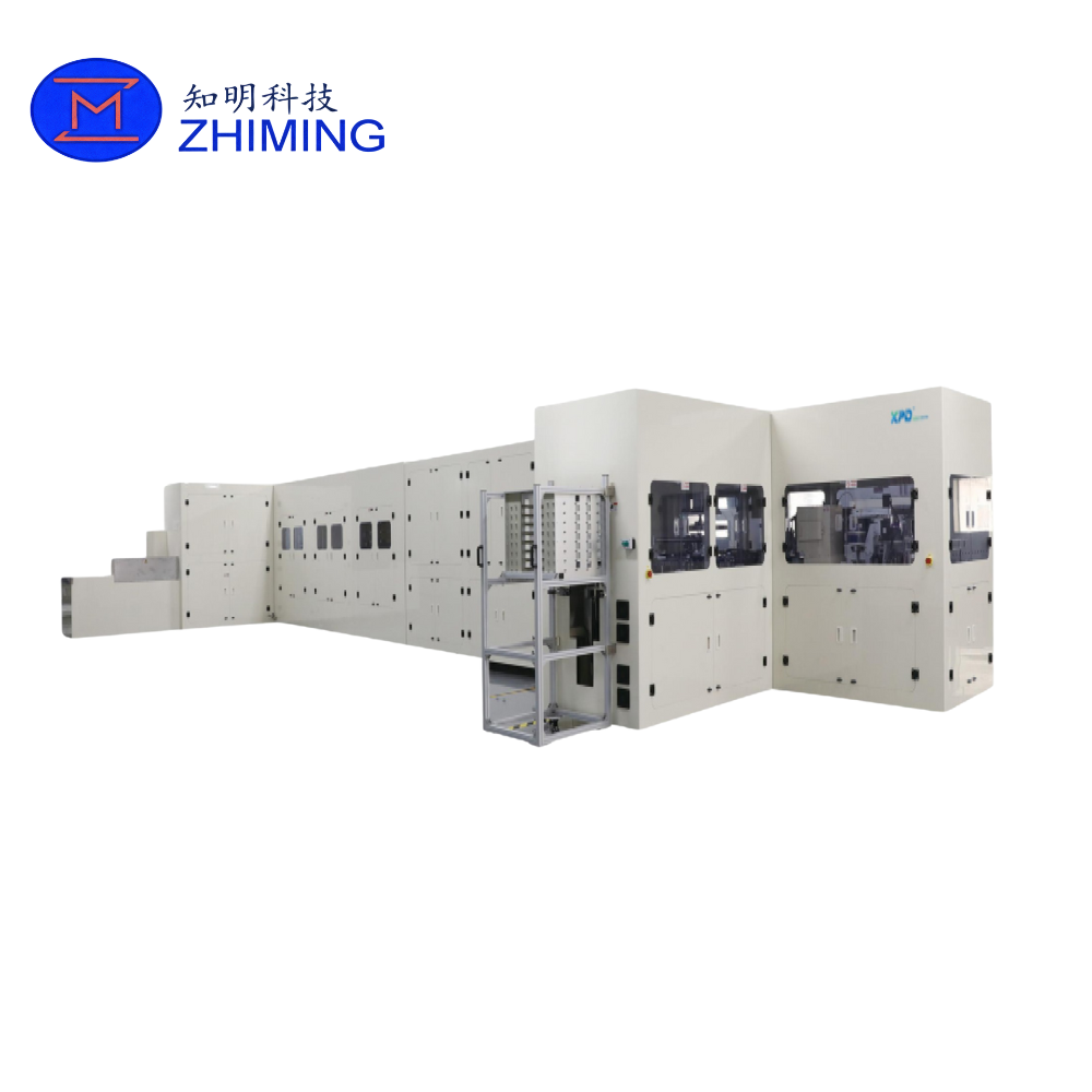
Product Overview
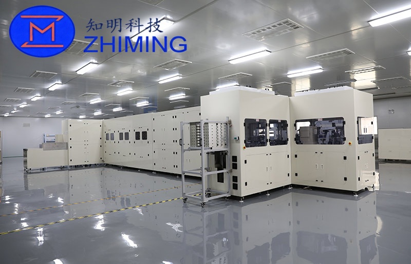
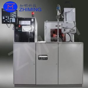
The 6–8 Inch Silicon & SiC Wafer Quad-Polishing Automation Line with Cleaning and Re-Mounting Loop is a fully integrated post-polishing process platform designed to support high-volume manufacturing of silicon and silicon carbide wafers.
The system connects quad-head polishing, automatic wafer de-mounting, ceramic carrier handling, carrier cleaning, and precision wafer re-mounting into a continuous closed-loop flow, eliminating manual handling and ensuring maximum process stability, repeatability, and yield.
It is optimized for power semiconductor wafers, SiC substrates, and advanced packaging applications where flatness, surface integrity, and contamination control are critical.
Closed-Loop Process Concept
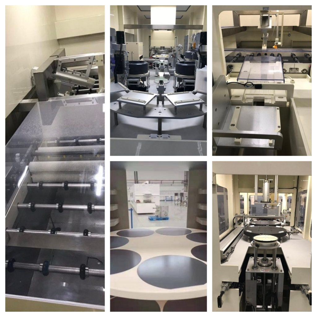
Unlike traditional semi-manual polishing lines, this system operates as a true closed-loop carrier cycle:
Polishing → De-mounting → Carrier Cleaning → Re-mounting → Polishing
Ceramic carriers circulate automatically inside the system, while wafers are precisely removed and re-mounted under tightly controlled conditions.
This architecture ensures that every polishing cycle starts with:
-
A clean carrier surface
-
A precisely positioned wafer
-
A stable and repeatable mounting interface
The result is lower wafer breakage, improved thickness uniformity, and higher batch-to-batch consistency.
Process-Critical Engineering Design
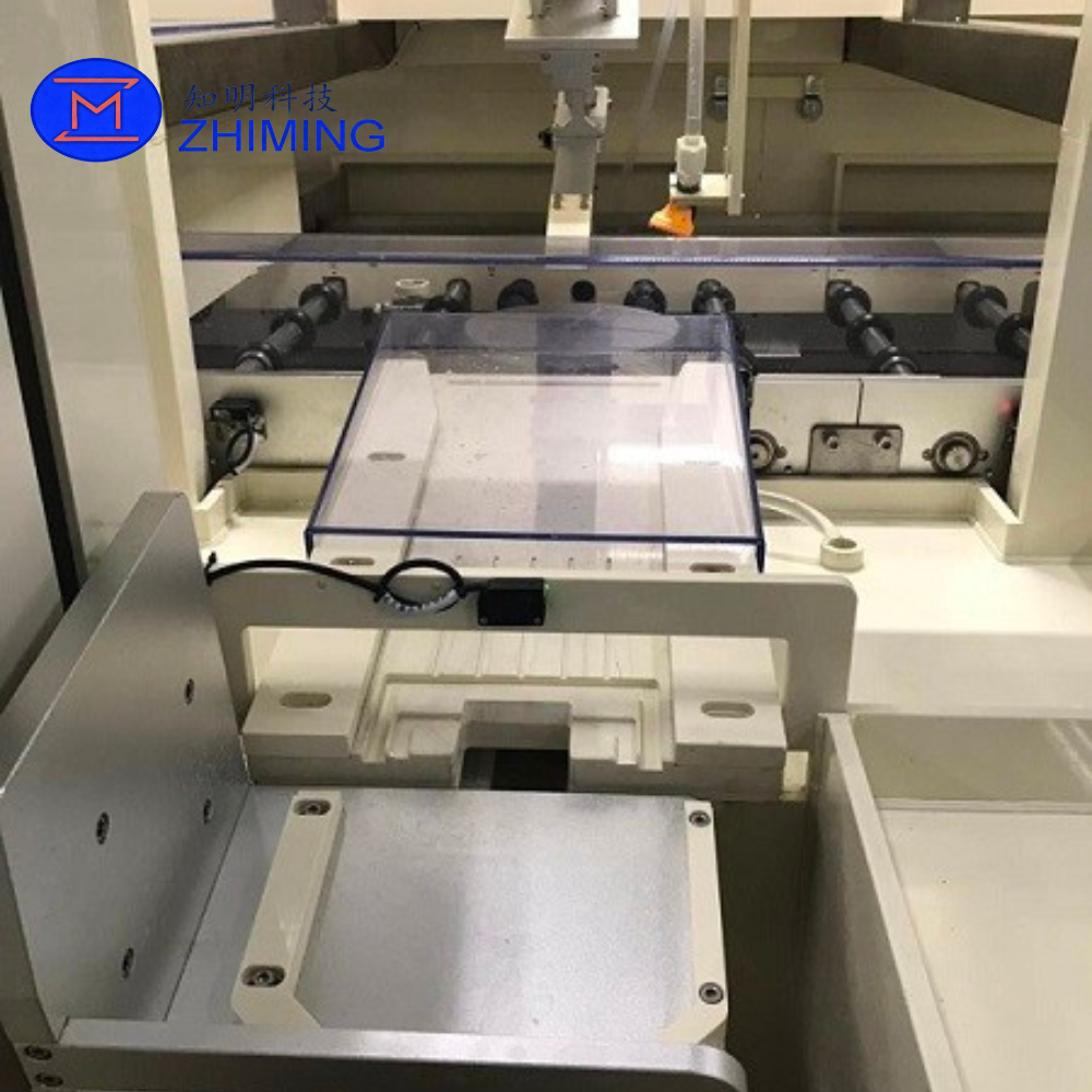
Low-Stress Wafer Handling
Special motion profiles and de-mounting trajectories are used to control acceleration, contact force, and separation angle, reducing:
-
Edge chipping
-
Micro-cracks
-
Stress-induced wafer warpage
This is especially important for SiC wafers, which are hard, brittle, and highly sensitive to mechanical shock.
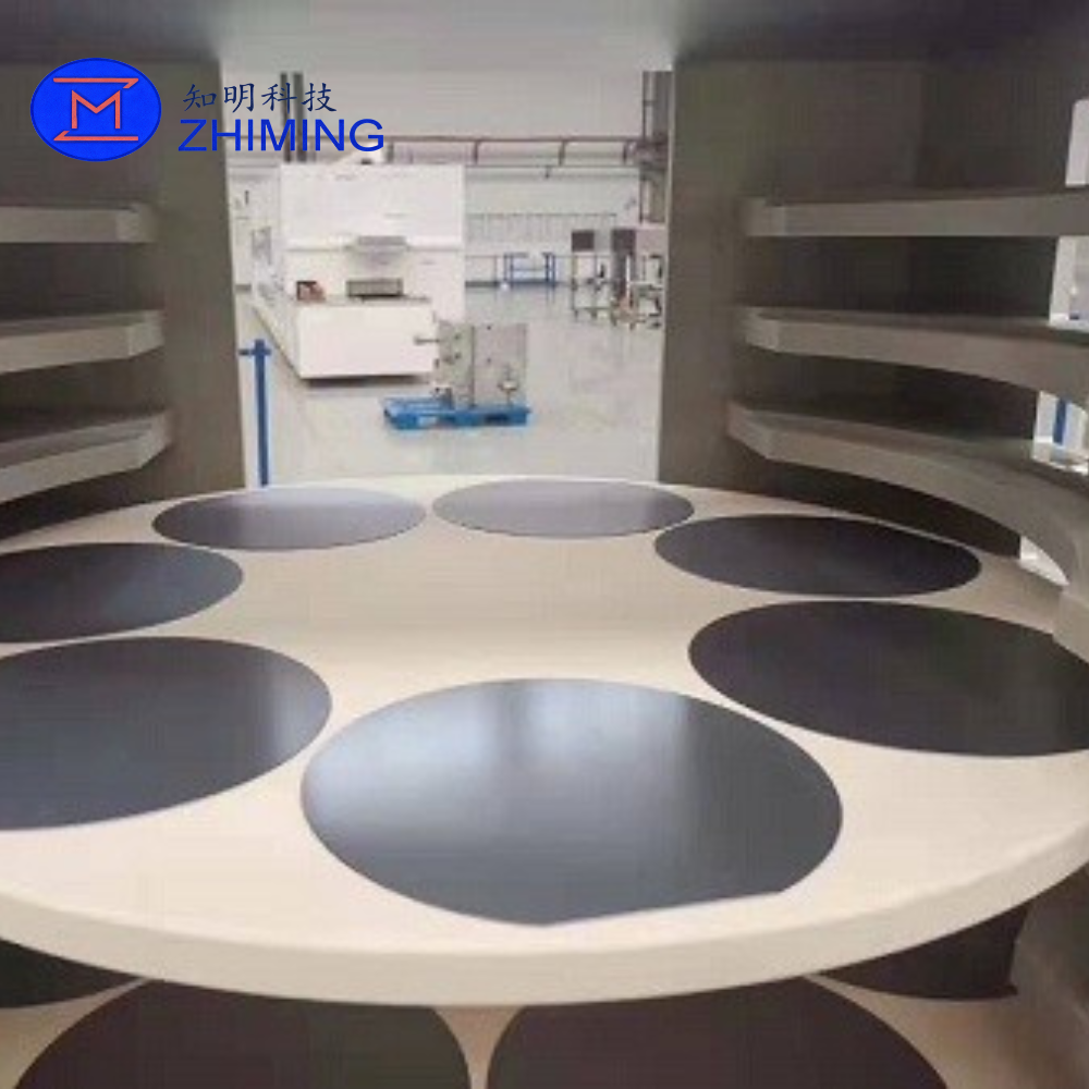
Ultra-Clean Carrier Reconditioning
Before each re-mounting cycle, ceramic carriers are restored to a process-ready surface state by removing slurry residues, fine particles, and chemical films.
This prevents:
-
Particle-induced scratches
-
Local polishing non-uniformity
-
Random surface defects
which are major yield killers in CMP and quad-polishing operations.
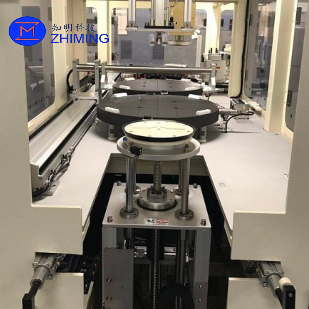
Precision Re-Mounting for Uniform Polishing
The re-mounting unit controls:
-
Mounting pressure
-
Wafer alignment
-
Flatness across the entire carrier
This guarantees that all wafers experience uniform polishing pressure during the next quad-polishing cycle, leading to:
-
Improved TTV (Total Thickness Variation)
-
Better surface roughness
-
Higher usable wafer yield
Production Flexibility
The system supports multiple wafer and carrier configurations, allowing fabs to tune the line for:
-
Maximum throughput
-
Maximum flatness control
-
Mixed 6-inch and 8-inch production
This makes the line suitable for both:
-
High-volume power device production
-
High-value SiC substrate processing
Typical Applications
-
Si and SiC power semiconductor wafers (MOSFETs, IGBTs, diodes)
-
SiC substrates and epitaxial wafers
-
Advanced packaging wafers
-
High-precision polished silicon wafers
FAQ – Additional Technical Questions
Q1: How does the system minimize wafer breakage for brittle SiC wafers?
The line uses low-stress de-mounting algorithms and controlled motion profiles, carefully managing acceleration, separation angle, and contact force. This prevents edge chipping, micro-cracks, and stress-induced wafer warpage, which are common issues with SiC substrates.
Q2: Can the cleaning and re-mounting loop handle multiple carrier specifications?
Yes. The carrier buffer and cleaning modules support multiple ceramic carrier diameters (e.g., 485 mm and 576 mm) and wafer counts per carrier. This allows mixed-size 6-inch and 8-inch wafer production without line interruption.
Q3: How does the system ensure repeatable polishing quality across batches?
By combining ultra-clean carrier surfaces, precision wafer alignment, and flatness control, each wafer is mounted under identical conditions. This guarantees consistent polishing pressure, uniform material removal, and minimal TTV, resulting in stable yield and surface quality across production batches.

Reviews
There are no reviews yet.