
In the rapidly evolving field of precision manufacturing, lasers have become indispensable tools for micro-drilling applications. Whether it’s creating microvias in printed circuit boards, drilling holes in sapphire or silicon carbide substrates, or machining delicate semiconductor wafers, lasers offer a level of precision and control that conventional mechanical tools cannot match. Yet, not all lasers are created equal. Choosing the right laser—picosecond (ps) or nanosecond (ns)—can mean the difference between flawless results and costly defects.
This article explores the fundamental differences between picosecond and nanosecond lasers, their impact on material processing, and practical guidelines to select the right laser for your micro-drilling needs.
Understanding Pulse Duration: Picoseconds vs. Nanoseconds
The primary difference between these two laser types lies in pulse duration:
- Nanosecond lasers (ns lasers) deliver energy in pulses lasting one-billionth of a second (10⁻⁹ s).
- Picosecond lasers (ps lasers) emit pulses lasting one-trillionth of a second (10⁻¹² s)—a thousand times shorter than nanosecond pulses.
Why does this matter? The shorter the pulse, the less heat is transferred to the surrounding material. In micro-drilling, this translates into minimal thermal damage, higher precision, and cleaner edges.
Thermal Effects: Why Heat Is the Invisible Enemy
In micro-drilling, precision is everything. However, unwanted heat can lead to:
- Burr formation
- Cracking or chipping in brittle materials
- Heat-affected zones (HAZ) that compromise material integrity
Nanosecond lasers, due to their longer pulses, tend to deposit more heat into the material. This makes them suitable for less brittle, thicker substrates, where drilling speed is more important than ultra-fine quality.
Picosecond lasers, on the other hand, confine energy to the target area in ultra-short bursts. The surrounding material remains nearly untouched—a process often called “cold ablation”—ideal for fragile, high-value, or thin substrates, including sapphire, SiC, and semiconductor wafers.
Material Considerations: Matching Lasers to Substrates
Different materials respond differently to laser pulses:
- Sapphire: Nanosecond lasers can drill, but risk microcracks; picosecond lasers minimize chipping and thermal stress.
- Silicon Carbide (SiC): Nanosecond lasers are effective for standard thicknesses; picosecond lasers are preferred for thin wafers or high-precision microholes to protect electrical properties.
- Metals (steel, copper, aluminum): Nanosecond lasers excel for high-throughput drilling; picosecond lasers are generally slower and used only when extreme precision or surface finish is critical.
- Polymers and thin films: Both ns and ps lasers can be effective; selection depends on the balance between speed and surface smoothness.
Insight: Picosecond lasers dominate in brittle, thin, or heat-sensitive materials, while nanosecond lasers shine in high-speed, bulk material processing.
Precision vs. Throughput: The Trade-Off
- Nanosecond lasers: High material removal rate, excellent for larger holes and thicker materials, but edges are rougher and microcracks can occur.
- Picosecond lasers: Lower throughput due to ultra-short pulses and smaller spot sizes, but holes are cleaner, edges smoother, and no recast layer forms.
A useful analogy: nanosecond lasers are like chisels—fast but rough, while picosecond lasers are scalpels—slow but precise.
Cost and Maintenance: Practical Considerations
Picosecond lasers are advanced systems with higher initial costs and more demanding maintenance due to precision optics. Nanosecond lasers are robust, cost-effective, and easier to maintain, making them suitable for large-scale production.
When deciding, consider:
- Required precision
- Production speed
- Material sensitivity
- Budget constraints
Rule of thumb: For fragile, high-value substrates, the upfront cost of a picosecond laser is justified by reduced defects and scrap. For durable, thicker materials, nanosecond lasers offer excellent cost-performance balance.
Typical Applications
Picosecond laser applications:
- Microvias in printed circuit boards
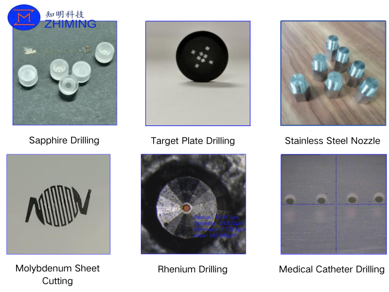
- Micro-hole drilling in sapphire and SiC substrates for LEDs
- Microholes in semiconductor wafers
- Precision ceramic components
Nanosecond laser applications:
- Drilling cooling holes in metals
- High-throughput plastic or polymer processing
- Rapid prototyping for thicker substrates
Key Takeaways
- Pulse duration defines thermal impact: shorter pulses = minimal heat, higher precision.
- Material type matters: fragile, thin, or heat-sensitive materials benefit most from picosecond lasers.
- Throughput vs. quality trade-off: nanosecond lasers = fast, picosecond lasers = ultra-clean.
- Cost and maintenance: picosecond lasers require higher investment but reduce defects; nanosecond lasers are economical and durable.
Conclusion
Selecting the right laser for micro-drilling is not just a technical detail—it’s a strategic decision. For high-value, fragile, or thin substrates like sapphire, SiC, and semiconductor wafers, picosecond lasers are nearly indispensable. For thicker, robust materials where speed matters more than ultra-fine precision, nanosecond lasers remain a highly efficient and cost-effective solution.
In short: the right pulse duration transforms micro-drilling from a risky process into a precise, reliable operation—because in laser machining, time truly is everything.