
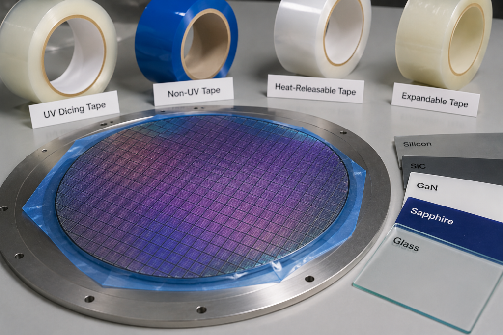
Wafer dicing tape is a temporary adhesive film used to hold a wafer securely during cutting, grinding, cleaning and die separation. Although it appears to be a simple consumable, its performance can directly affect die movement, edge chipping, contamination, wafer breakage and final pick-up yield.
The correct tape must provide enough adhesion to keep the wafer and individual dies stable during dicing. At the same time, it must allow the finished dies to be removed without excessive force, adhesive residue or damage.
Different semiconductor materials behave differently during dicing. Silicon, silicon carbide, sapphire, glass, gallium nitride and other materials vary in hardness, brittleness, thickness, surface finish and sensitivity to stress. As a result, one tape type is not suitable for every wafer.
This guide explains how to select wafer dicing tape according to wafer material, dicing method, die size, process temperature and downstream handling requirements.
What Is Wafer Dicing Tape?
Wafer dicing tape is an adhesive film mounted on a metal or plastic frame. The wafer is attached to the tape before being cut into individual dies.
During dicing, the tape performs several functions:
- Holds the wafer in a fixed position
- Prevents dies from moving after separation
- Supports thin or fragile wafers
- Reduces die loss during water cleaning
- Maintains die spacing
- Supports automatic die pick-up
- Protects the wafer backside
- Helps reduce mechanical vibration
After dicing, the adhesive force may be reduced by ultraviolet exposure, thermal treatment or controlled tape expansion, depending on the tape type.
Why Tape Selection Matters
An unsuitable tape can cause serious process problems.
If the adhesion is too low, dies may shift, rotate or detach during cutting. If the adhesion is too high, the die may crack during pick-up or retain adhesive residue.
Poor tape selection can result in:
- Die flying
- Wafer displacement
- Backside contamination
- Adhesive residue
- Difficult die pick-up
- Die cracking
- Szélek forgácsolódása
- Tape cutting
- Water penetration
- Frame distortion
- Reduced production yield
The most appropriate tape is selected by balancing holding strength, release performance, cleanliness and mechanical support.
Main Types of Wafer Dicing Tape
Wafer dicing tapes can be divided into several general categories.
Standard Pressure-Sensitive Dicing Tape
Standard pressure-sensitive adhesive tape maintains relatively stable adhesion before and after dicing.
It is often used for:
- General silicon wafers
- Larger dies
- Thicker wafers
- Low-risk dicing processes
- Applications that do not require UV release
Advantages include simple handling and relatively low cost.
However, strong permanent adhesion may make small or thin dies difficult to remove.
UV-Releasable Dicing Tape
UV dicing tape provides relatively strong adhesion during processing. After dicing, the tape is exposed to ultraviolet light, which reduces its adhesive strength.
This allows the dies to be picked up more easily.
UV-release tape is commonly used for:
- Small semiconductor dies
- Thin wafers
- Fragile dies
- High-density die layouts
- Automated die bonding
- High-value devices
The UV exposure energy, wavelength and exposure uniformity must be controlled to achieve consistent release.
Non-UV or Low-Tack Tape
Low-tack tapes are designed for applications where strong adhesion is unnecessary or where the wafer surface is highly sensitive.
They may be suitable for:
- Large dies
- Thick wafers
- Low-cutting-force processes
- Sensitive backside coatings
- Temporary laboratory work
Their main limitation is the increased risk of die movement or detachment.
Heat-Releasable Tape
Heat-release tape loses adhesion after being exposed to a specified temperature.
It may be used when UV exposure is unavailable or undesirable.
However, the required release temperature must be compatible with:
- Wafer materials
- Metallizálás
- Polymer layers
- Temporary bonding materials
- Device structures
Expandable Dicing Tape
Expandable tape is designed to stretch after dicing, increasing the distance between individual dies.
Tape expansion can:
- Improve die separation
- Support optical inspection
- Reduce die-to-die contact
- Make robotic pick-up easier
- Help separate small dies
The tape must expand evenly to prevent die displacement or pattern distortion.
Key Parameters for Selecting Dicing Tape
Several tape properties should be evaluated before use.
Initial Adhesion
Initial adhesion determines how firmly the wafer is held before and during cutting.
The required adhesion depends on:
- Wafer diameter
- Wafer thickness
- Die size
- Cutting speed
- Spindle speed
- Cooling-water pressure
- Blade condition
- Wafer material
- Dicing method
Hard and brittle materials often require stable holding because they may generate greater vibration or cutting resistance.
Adhesion After UV Exposure
For UV tape, the post-UV adhesion must be low enough for die pick-up but not so low that the dies shift before unloading.
Incomplete UV exposure may result in uneven release across the wafer.
Base Film Thickness
The base film provides mechanical support and influences blade penetration.
A thicker film can provide greater support but may:
- Increase cutting resistance
- Require deeper blade penetration
- Increase the risk of blade wear
- Affect tape expansion
A thinner film may reduce support for fragile or thin wafers.
Adhesive Thickness
Adhesive thickness affects surface conformity and holding strength.
A thicker adhesive layer may improve contact with rough surfaces, but it can increase the risk of adhesive transfer or blade contamination.
Tape Stiffness
Tape stiffness influences wafer support, frame handling and expansion behavior.
A very flexible tape may deform during cutting, while an overly stiff film may not conform well to warped or uneven wafers.
Heat Resistance
The tape must withstand any process temperature encountered during:
- Wafer mounting
- Dicing
- Drying
- Tisztítás
- UV-expozíció
- Temporary storage
- Die bonding preparation
Excessive heat may cause adhesive flow, residue or loss of holding strength.
Water Resistance
Blade dicing normally uses deionized water for cooling and debris removal.
The adhesive must resist:
- Water penetration
- Edge lifting
- Adhesion loss
- Swelling
- Contamination
This is especially important during long dicing cycles.
Cleanliness and Residue
For semiconductor and optical applications, low residue is critical.
Residual adhesive can interfere with:
- Die bonding
- Wire bonding
- Backside metallization
- Optical surfaces
- Thermal interfaces
- Packaging reliability
Tape selection should consider both visible residue and trace organic contamination.
Selecting Tape for Silicon Wafers
Silicon is the most widely processed semiconductor wafer material. It is relatively well understood and can be diced using blade, laser or stealth methods.
Standard silicon wafers generally offer more tape flexibility than extremely hard or highly brittle materials.
Suitable Tape Characteristics
For standard silicon wafer dicing, the tape should provide:
- Moderate and stable adhesion
- Good water resistance
- Clean release
- Compatibility with automated pick-up
- Sufficient support for the selected thickness
UV-release tape is often selected when the dies are small, thin or densely arranged.
Thick Silicon Wafers
Thicker silicon wafers and large dies may be processed with standard non-UV tape because the risk of die deformation during pick-up is relatively low.
Thin Silicon Wafers
Thin silicon wafers require more careful support.
The tape should:
- Minimize wafer bowing
- Prevent local movement
- Reduce backside stress
- Release with low pick-up force
UV tape is usually advantageous for thin wafers because the adhesion can be reduced before die removal.
Small Silicon Dies
Small dies have limited surface area for pick-up tools and may be difficult to separate from high-tack adhesive.
A UV-releasable tape with uniform post-exposure release is generally preferred.
Selecting Tape for Silicon Carbide Wafers
Silicon carbide is much harder than silicon and is commonly used for power electronic and high-temperature devices.
SiC dicing may produce high cutting forces, blade wear and edge chipping. The tape must hold the wafer and separated dies securely throughout the process.
Recommended Tape Properties
Suitable tape for SiC wafers should provide:
- Strong initial adhesion
- High mechanical stability
- Good resistance to cutting water
- Low film deformation
- Clean release after dicing
- Support for hard-material cutting conditions
UV-release tape is frequently useful because it combines strong holding during cutting with lower adhesion during pick-up.
Why Stronger Holding May Be Required
The high hardness of SiC can increase:
- Blade load
- Process vibration
- Cutting time
- Local stress
- Risk of die movement
Insufficient adhesion may result in die rotation or detachment after the cut is completed.
Thin SiC Wafers
Thin SiC wafers are both valuable and fragile. Tape mounting must avoid air bubbles, particles and uneven pressure.
A tape that is too soft may permit local bending, while a tape with excessive post-process adhesion may crack the die during removal.
Selecting Tape for Glass Wafers
Glass wafers are used in sensors, microfluidics, MEMS, optical devices and advanced packaging.
Glass is brittle and sensitive to edge defects. During dicing, it may produce chips, particles and microcracks.
Recommended Tape Properties
Tape for glass wafer dicing should offer:
- Uniform surface contact
- Strong resistance to water
- Stable support under brittle cutting conditions
- Alacsony szennyezettség
- Controlled release
- Good particle retention
Surface Smoothness
Smooth glass generally provides good tape contact. However, coated, patterned or rough glass surfaces may require a different adhesive system.
The tape must conform to the backside without trapping air.
Transparent Materials and UV Exposure
When UV tape is used, the optical properties of the wafer and tape system should be considered.
Exposure may be performed through the tape side. The frame, backing material and equipment configuration must allow uniform ultraviolet treatment.
Glass Chipping Control
Tape cannot eliminate chipping by itself, but stable backside support can reduce vibration and prevent separated glass pieces from moving during cutting.
Selecting Tape for Sapphire Wafers
Sapphire is extremely hard and brittle. It is used for LED substrates, optical components, RF devices and protective windows.
Dicing sapphire can create considerable cutting stress and edge damage.
Suitable Tape Characteristics
Tape for sapphire should provide:
- High initial holding strength
- Stable support during long dicing cycles
- Resistance to cooling water
- Low film stretching
- Reliable UV release
- Minimal residue
The tape must remain stable even when dicing speed is reduced or multiple cutting passes are required.
Die Pick-Up Considerations
Sapphire dies and optical parts may have polished surfaces that are sensitive to scratches and contamination.
Post-UV adhesion should be low enough to avoid excessive pick-up force.
For optical components, adhesive cleanliness is particularly important because residue can affect later cleaning and coating processes.
Selecting Tape for Gallium Nitride Wafers
GaN devices may be manufactured on sapphire, silicon, silicon carbide or freestanding GaN substrates.
Tape selection therefore depends not only on the active material but also on the substrate structure.
GaN-on-Sapphire
GaN-on-sapphire wafers typically require tape suitable for hard, brittle sapphire substrates.
A legfontosabb követelmények a következők:
- Strong holding during cutting
- Good particle control
- Low post-UV adhesion
- Compatibility with small LED dies
- Stable tape expansion
GaN-on-Silicon
GaN-on-silicon wafers may use tape systems similar to silicon processing, although wafer stress, layer structure and die size still need to be considered.
Freestanding GaN
Freestanding GaN wafers can be expensive and brittle. Low-stress mounting and carefully controlled release are critical.
Selecting Tape for Gallium Arsenide and Indium Phosphide
GaAs and InP are compound semiconductor materials used in RF, photonic, laser and high-speed electronic devices.
Compared with silicon, these materials are generally more brittle and may require more careful handling.
Recommended Tape Properties
The tape should provide:
- Strong but uniform support
- Alacsony szennyezettség
- Low release force after dicing
- Good compatibility with thin wafers
- Reliable holding of small dies
- Minimal adhesive transfer
UV tape is often preferred for small photonic and RF dies.
Surface Sensitivity
Backside metallization or thin films may be present. The adhesive chemistry must be compatible with these layers.
A tape suitable for bare semiconductor material may not be suitable for a wafer with plated, polymer-coated or textured backside surfaces.
Selecting Tape for Ceramic and Advanced Substrates
Dicing tape is also used for alumina, aluminum nitride, LTCC and other ceramic substrates.
These materials may be harder or rougher than standard semiconductor wafers.
Tape selection should consider:
- Surface roughness
- Substrate thickness
- Cutting force
- Die weight
- Water exposure
- Részecskék keletkezése
- Pick-up method
A thicker adhesive layer may improve contact with a slightly rough surface, but it can also increase residue risk.
Influence of Wafer Thickness
Wafer thickness is one of the most important tape-selection factors.
Thick Wafers
Thick wafers are mechanically stable but may require deeper blade penetration.
The tape must be thick enough to protect the frame and allow proper overcut without excessive blade contact.
Thin Wafers
Thin wafers require greater support because they can:
- Íj
- Warp
- Crack
- Move during cutting
- Break during handling
Tape for thin wafers should provide uniform adhesion and low release force.
Ultra-Thin Wafers
Ultra-thin wafers may require specialized tapes and temporary bonding processes.
In some cases, dicing is performed before grinding or with the wafer attached to a carrier.
The tape must be selected together with the complete thinning and dicing process rather than as an isolated consumable.
Influence of Die Size
Large and small dies impose different requirements.
Large Dies
Large dies have greater adhesive contact area, which can make removal difficult.
Even moderate adhesive strength may produce high total pick-up force.
Small Dies
Small dies are more likely to:
- Shift
- Rotate
- Fly away
- Become difficult to detect
- Move during tape expansion
They require stable holding during cutting but low and consistent adhesion after release.
Influence of the Dicing Method
The selected dicing method also affects tape requirements.
Penge Dicing
Blade dicing introduces mechanical contact, vibration and cooling water.
Tape must provide:
- Water resistance
- Strong die retention
- Adequate base-film thickness
- Stable adhesion
- Compatibility with blade penetration
Lézeres aprítás
Laser dicing may create heat, debris and local material changes.
Tape must tolerate the laser process without:
- Melting
- Shrinking
- Outgassing
- Producing excessive residue
- Contaminating the optical path
Stealth Dicing
Stealth dicing forms a modified layer inside the wafer and separates dies through controlled stress or expansion.
The tape must support uniform expansion and die separation.
Tape elasticity and expansion consistency are especially important.
Plasma Dicing
Plasma dicing may involve mask materials, vacuum processing and chemically active environments.
Standard dicing tape may not be suitable unless it is protected from plasma exposure.
Specialized carrier and tape structures may be required.
Dicing Before Grinding
Dicing before grinding, also known as DBG, forms grooves in the wafer before backside thinning.
Tape selection must support the wafer through multiple process stages and maintain dimensional stability.
The tape system may need to tolerate:
- Grinding forces
- Water
- Tisztítás
- Thin-wafer handling
- Die separation
Common Tape-Related Dicing Problems
Die Flying
Die flying occurs when a die detaches during cutting or cleaning.
Possible tape-related causes include:
- Insufficient initial adhesion
- Poor wafer-to-tape contact
- Water penetration
- Contaminated wafer backside
- Excessive cutting force
- Incorrect tape aging
Difficult Die Pick-Up
High pick-up force may be caused by:
- Excessive adhesive strength
- Incomplete UV exposure
- Incorrect UV dose
- Large die area
- High adhesive thickness
- Tape not designed for the die size
Adhesive Residue
Residue may result from:
- Incompatible adhesive chemistry
- Excessive temperature
- Long storage after mounting
- Excessive pressure during lamination
- Inadequate UV exposure
- Rough wafer backside
Tape Peeling or Edge Lifting
Possible causes include:
- Poor frame mounting
- Low water resistance
- Contaminated surfaces
- Incorrect lamination pressure
- Warped wafers
- Improper tape tension
Tape Cutting
If the blade penetrates too deeply, it may cut through the tape.
This can cause:
- Frame contamination
- Die movement
- Blade damage
- Water leakage
- Poor tape expansion
Blade depth and base-film thickness must be coordinated.
Uneven Tape Expansion
Uneven expansion can disturb die spacing and create pick-up errors.
Possible causes include:
- Uneven frame mounting
- Nonuniform tape stiffness
- Incorrect expansion temperature
- Asymmetric die layout
- Damaged film
- Excessive residual adhesion
Wafer Mounting Best Practices
Correct mounting is as important as tape selection.
Before mounting:
- Clean the wafer backside
- Remove particles and moisture
- Confirm tape shelf life
- Inspect the tape surface
- Check the mounting frame
- Verify tape compatibility
During mounting:
- Apply uniform pressure
- Avoid trapped air
- Prevent wrinkles
- Maintain correct tension
- Control lamination speed
- Avoid direct contact with optical surfaces
After mounting:
- Inspect for bubbles
- Confirm wafer centering
- Check edge adhesion
- Allow the adhesive to stabilize if required
- Avoid excessive storage time before dicing
UV Exposure Considerations
For UV-release tape, consistent exposure is essential.
Important parameters include:
- UV wavelength
- Exposure intensity
- Total energy
- Exposure duration
- Distance from the lamp
- Lamp uniformity
- Tape transparency
- Frame shadowing
Underexposure can leave the tape too adhesive. Overexposure may reduce adhesion excessively or affect certain polymer materials.
UV equipment should be regularly calibrated.
Cleanroom and Storage Requirements
Dicing tape should be stored according to the manufacturer’s recommended conditions.
Factors that can affect tape performance include:
- Hőmérséklet
- Humidity
- Light exposure
- Shelf life
- Dust
- Packaging damage
- Chemical contamination
Tape should remain sealed until use and should not be used after its validated storage period.
Questions to Ask a Dicing Tape Supplier
Before selecting a tape, engineers should ask:
- What wafer materials is the tape designed for?
- Is it UV-releasable, heat-releasable or permanent tack?
- What is the initial adhesion?
- What is the adhesion after UV exposure?
- What UV dose is required?
- What is the base-film thickness?
- What is the adhesive thickness?
- Is the tape resistant to deionized water?
- What temperature range can it tolerate?
- Is it suitable for thin wafers?
- Is it compatible with tape expansion?
- What residue level is expected?
- Is it approved for backside metallization?
- What die-size range is recommended?
- What storage conditions are required?
Practical Selection Table
| Wafer Material | Main Processing Risk | Recommended Tape Characteristics |
|---|---|---|
| Szilícium | Die movement, pick-up force | Moderate adhesion, clean release, UV option for thin or small dies |
| Szilícium-karbid | High cutting force, chipping | Strong initial adhesion, high stability, UV release |
| Glass | Brittleness, particles, water exposure | Uniform support, water resistance, controlled release |
| Zafír | Hardness, long cutting time, edge damage | High holding strength, low stretch, clean UV release |
| GaN-on-sapphire | Small dies, brittle substrate | Strong retention, expansion stability, low post-UV tack |
| GaAs | Fragility, backside sensitivity | Low-stress support, low residue, UV release |
| InP | High brittleness, small photonic dies | Uniform adhesion, low pick-up force, clean release |
| Ceramic substrates | Roughness, high cutting load | Good conformability, strong support, water resistance |
How to Qualify a New Dicing Tape
A new tape should be tested under actual process conditions before full production use.
A qualification trial may evaluate:
- Wafer mounting quality
- Initial adhesion
- Dicing stability
- Die movement
- Szélek forgácsolódása
- Tape damage
- Water resistance
- UV release
- Pick-up force
- Adhesive residue
- Die-bonding compatibility
- Tape expansion uniformity
- Final yield
The test should use representative wafer material, thickness, die size, blade type and process parameters.
Gyakran ismételt kérdések
Is UV tape always better than standard dicing tape?
No. UV tape is useful when strong holding and easy die release are both required. Standard tape may be sufficient for thick wafers, large dies or simple laboratory processes.
What tape is best for silicon carbide wafers?
SiC generally requires tape with strong initial adhesion, good water resistance and high mechanical stability. UV release is often preferred to reduce pick-up force after dicing.
Can the same tape be used for silicon and sapphire?
Sometimes, but the process requirements are different. Sapphire normally generates higher cutting loads and may require stronger support and better dimensional stability.
Why do dies remain difficult to pick up after UV exposure?
Possible reasons include insufficient UV energy, shadowing, incorrect lamp wavelength, expired tape or an adhesive that is not suitable for the die size.
Can dicing tape reduce wafer chipping?
Tape cannot fully prevent chipping, but stable wafer support can reduce vibration and die movement. Blade condition, feed speed, spindle speed and cooling-water control are also important.
Does tape thickness affect blade dicing?
Yes. The blade normally penetrates slightly into the tape. A tape that is too thin increases the risk of cutting through it, while excessive thickness may affect cutting behavior.
How long can a wafer remain mounted on dicing tape?
The allowable time depends on the adhesive system, wafer surface, temperature and storage conditions. Long mounting periods can increase adhesion or residue risk.
Is low-tack tape suitable for thin wafers?
Not always. Thin wafers require uniform support and may shift if adhesion is too low. A UV tape that provides strong initial adhesion and low post-exposure tack is often more suitable.
Következtetés
Wafer dicing tape selection should be treated as part of the complete dicing process rather than as a simple purchasing decision.
The correct tape depends on:
- Wafer material
- Wafer thickness
- Die size
- Dicing method
- Cutting force
- Cooling-water exposure
- Backside surface condition
- Pick-up method
- Cleanliness requirements
- Tape expansion requirements
Silicon may tolerate a broad range of tape systems, while SiC and sapphire generally require stronger and more stable holding. Glass and compound semiconductor wafers require careful control of stress, contamination and release force.
Before volume production, the selected tape should be qualified using the actual wafer, die layout and dicing parameters. A well-matched dicing tape can improve die stability, reduce damage, simplify pick-up and increase overall manufacturing yield.