
In the rapidly advancing semiconductor and optoelectronic industries, the precision and efficiency of wafer fabrication directly determine the cost and performance of downstream devices. With the widespread adoption of 12-inch (300 mm) large-diameter wafers, traditional slicing methods face increasingly critical challenges: high material loss, surface roughness, micro-cracks, and production speeds that struggle to meet mass manufacturing demands. In recent years, the introduction of diamond wire saw (DWS) technology has sparked an “efficiency revolution,” redefining the standards of wafer slicing.
1. Principle of Diamond Wire Saw Technology
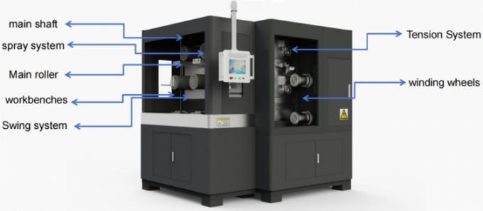
At the core of diamond wire saw technology is a high-strength steel or alloy wire uniformly coated with ultra-hard diamond particles. During slicing, the wire moves at high speed—either in reciprocating or continuous motion—producing micro-scale cutting action along the wafer surface to separate silicon ingots or rods into thin slices. Unlike conventional multi-wire saws, DWS combines the effects of “abrasion and cutting,” which reduces mechanical stress and minimizes cutting damage, resulting in higher wafer integrity.
2. Challenges in Slicing 12-Inch Wafers
As wafer diameters increase from 8 inches to 12 inches, the volume and weight rise by approximately 2.25 times. Traditional wire saws and circular saws are prone to bending, breakage, or thermal stress concentration during large-diameter wafer cutting. Additionally, modern applications demand ever-thinner wafers, sometimes below 150 µm, imposing stricter requirements on slicing precision and surface quality. Micro-cracks and edge chipping not only lower yield but can also trigger failures in subsequent processes. Consequently, precise control at the microscopic cutting level becomes a critical bottleneck for mass-producing 12-inch wafers.
3. Dual Advantages: Efficiency and Precision
The greatest strength of DWS lies in its ability to achieve high cutting speed without compromising precision. By optimizing diamond particle size, coating uniformity, and wire speed, modern DWS systems can achieve the following breakthroughs:
- Low material loss: Thin wire and uniform abrasion reduce wafer kerf to 0.05–0.08 mm per slice, lowering material waste by 30–40% compared to traditional multi-wire saws.
- High surface quality: Sliced surface roughness reaches Ra 0.2–0.3 µm, significantly reducing subsequent polishing requirements.
- Micro-crack control: Uniform cutting stress distribution minimizes edge chipping, improving the yield of ultra-thin wafers.
- Fast slicing speed: Cutting a 12-inch wafer can be completed in 1.5–2 hours, compared to several hours with traditional methods, significantly boosting production efficiency.
Moreover, automated tension control, depth monitoring, and coolant circulation ensure stability and repeatability, providing reliable support for large-scale wafer production.
4. Technological Innovation and Industry Value
DWS is not merely an equipment upgrade; it represents a paradigm shift in wafer manufacturing. By integrating material science, precision mechanical control, and automated monitoring, it achieves “low-loss, high-yield, high-throughput” slicing. In fields such as semiconductor chips, photovoltaic wafers, and power devices, DWS reduces raw material costs, enhances device performance, and shortens the cycle from research to mass production. Particularly in power semiconductors and next-generation photovoltaic applications, the ability to slice 12-inch wafers at scale will become a key competitive advantage.
5. Future Trends
Future development of DWS technology is likely to focus on higher intelligence, ultra-low loss, and multifunctionality:
- Intelligent control: AI-based algorithms can monitor cutting parameters in real time, achieving adaptive slicing and further improving yield.
- Ultra-low loss: Optimizing diamond particle shape and distribution allows wafer thicknesses below 100 µm while maintaining stability.
- Green manufacturing: Enhanced coolant recycling and debris recovery enable energy-efficient and environmentally friendly cutting.
- Multifunctionality: Combining wafer slicing with half-cut or custom geometries supports advanced power devices and composite materials.
In summary, the application of diamond wire saw technology in 12-inch wafer slicing is more than a tool upgrade; it symbolizes the semiconductor industry’s shift toward precision, intelligence, and high efficiency. This “efficiency revolution” not only reduces manufacturing costs but also drives comprehensive improvements in semiconductor materials and device performance, injecting new momentum into the optoelectronic, power electronics, and renewable energy sectors.