
The semiconductor manufacturing industry relies on a wide array of highly specialized equipment to produce advanced integrated circuits. This article provides an overview of eight critical categories of Halbleiterausrüstung, examining their functions, technological significance, and industry trends.
1. Lithography Equipment
Lithography machines are the cornerstone of semiconductor manufacturing. The lithography process defines the smallest feature sizes on chips and directly determines process nodes and device performance. Advanced chips often require 60 to 90 lithography steps, with lithography accounting for roughly 30% of manufacturing costs and 40–50% of total processing time.
A lithography system typically comprises a light source, uniform illumination optics, projection lenses, and precision mechanical and control systems, including wafer stages and mask aligners. As semiconductor complexity grows, domestic production of lithography systems is still limited, and much of the market relies on imported equipment. Current development efforts focus on achieving smaller nodes and higher precision, with ongoing progress in immersion lithography technologies.
2. Etching Equipment
Etching is a core process for transferring circuit patterns from masks onto wafers. Etching equipment removes material from the wafer surface to form precise microstructures required for integrated circuits. Etching processes are divided into dry etching and wet etching.
- Dry etching, which dominates over 90% of applications, includes plasma etching, ion sputtering, and reactive ion etching. It offers better anisotropy and precision for submicron features.
- Wet etching is typically used for larger features or post-dry-etch residue removal.
Dry etching can also be categorized into physical etching and chemical etching. Physical etching relies on ion bombardment, while chemical etching involves reactive plasmas that form volatile byproducts. These techniques are critical in logic and memory chip fabrication.
3. Thin-Film Deposition Equipment
Thin-film deposition equipment is essential for creating conductive or insulating layers on wafers. The main deposition techniques include:
- Chemical Vapor Deposition (CVD) – PECVD, LPCVD, APCVD, and SACVD variants allow deposition of silicon dioxide, silicon nitride, and other materials with high uniformity and low defect rates.
- Physical Vapor Deposition (PVD) – Mainly sputtering, used for metal layers in CMOS devices.
- Atomic Layer Deposition (ALD) – Enables ultra-thin, high-precision layers, critical for advanced nodes and 3D NAND structures.
With the growing complexity of 3D memory devices and FinFET structures, the demand for thin-film deposition equipment continues to rise, both domestically and internationally.
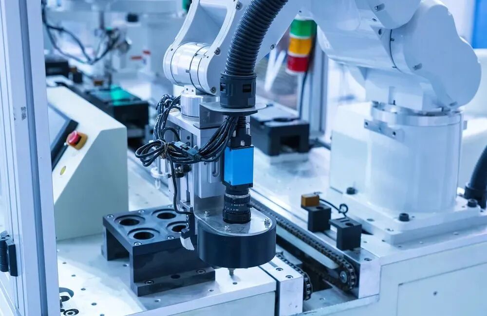
4. Metrology and Inspection Equipment
Metrology and inspection tools are crucial for maintaining high yields and reducing production costs.
- Metrology equipment measures wafer structures, thin-film thickness, critical dimensions, and surface morphology to ensure process compliance.
- Inspection equipment detects defects such as particles, scratches, or circuit anomalies to prevent yield loss.
The Chinese market has grown significantly in recent years, contributing an increasing share of the global semiconductor inspection equipment market.
5. Ion Implantation Equipment
Ion implantation is a key process for doping semiconductor wafers. It involves accelerating ions of specific elements into the wafer to precisely alter electrical properties. Advantages over traditional thermal diffusion doping include:
- High uniformity and controllability of dopant distribution
- Ability to selectively dope patterned areas
- No limitations imposed by material solubility
Ion implantation is widely applied in advanced logic, memory, and solar cell manufacturing. Domestic development has achieved significant milestones, covering full-process support for 12-inch wafers at advanced nodes.
6. Cleaning Equipment
Wafer cleaning ensures high yield and device performance by removing particles, residues, metals, and other contaminants. Cleaning equipment employs two main approaches:
- Wet cleaning – Uses chemical solutions and deionized water, often with ultrasonic or spray-assisted processes; it accounts for over 90% of cleaning steps.
- Dry cleaning – Uses gas-phase chemicals or plasma to remove specific contaminants, mainly applied in advanced nodes.
Cleaning technologies continue to evolve toward smaller footprints, higher efficiency, and environmentally friendly operation. The increasing complexity of 3D integrated circuits drives demand for sophisticated cleaning processes throughout wafer fabrication.
7. Chemical Mechanical Polishing (CMP) Equipment
CMP equipment performs global planarization of wafer surfaces by combining chemical etching with mechanical polishing. It ensures wafer flatness for subsequent etching or deposition processes and is critical in advanced packaging applications such as 2.5D/3D IC integration and TSV structures.
As device complexity and metal layer stacking increase, CMP becomes essential for maintaining uniformity, minimizing defects, and enabling high-resolution lithography.
8. Semiconductor Test Equipment
Testing ensures that semiconductor devices meet functional and electrical specifications. Test equipment includes:
- Testers – Evaluate performance and functionality of wafers and packaged chips.
- Probing stations – Connect wafers to testers for in-line testing.
- Sorters – Automate handling and classification of tested devices.
Testing represents a significant portion of equipment value, often exceeding 60%, highlighting its importance in the semiconductor value chain from wafer fabrication to final assembly.
Schlussfolgerung
The semiconductor equipment industry spans lithography, etching, deposition, metrology, ion implantation, cleaning, CMP, and testing segments. Technological advancement in each category is vital to achieving higher yields, smaller process nodes, and more complex devices. With domestic and international markets growing, ongoing innovation, automation, and precision will remain key drivers for the semiconductor equipment sector.