
The semiconductor industry is evolving at an unprecedented pace. As process nodes shrink from 7nm to 3nm and beyond, the demands on manufacturing equipment for precision, stability, and efficiency continue to rise. At the same time, global demand for smart, high-yield production has accelerated the trend toward higher precision and automation in semiconductor manufacturing equipment.
1. Enhanced Precision: Nanometer-Level Control
As transistor dimensions shrink, equipment precision becomes critical:
- Lithography tools: EUV lithography systems are already achieving nanometer-level resolution. Future nodes below 3nm will require even greater optical stability and minimal distortion.
- Etching equipment: Deep reactive ion etching (DRIE) and plasma etching must achieve higher anisotropy and uniformity to ensure wafer-wide yield.
- Thin-film deposition tools (CVD/ALD): Atomic-level thickness control is essential for advanced packaging and FinFET structures, with tolerances below 1 nanometer.
Key takeaway: Precision, stability, and repeatability will define the competitiveness of next-generation equipment.
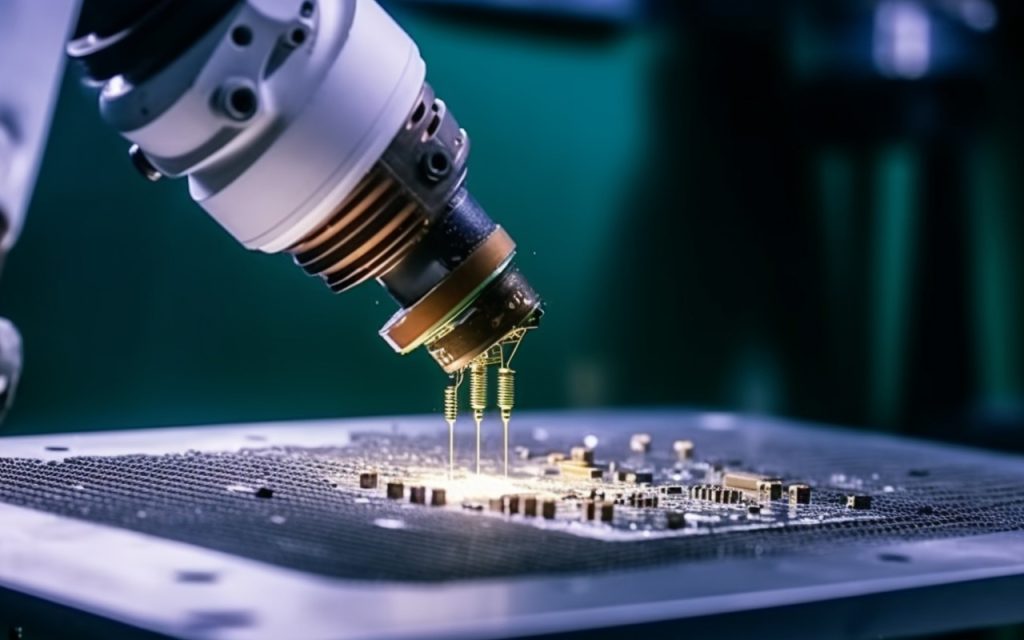
2. Automation and Smart Manufacturing
Traditional semiconductor production relies heavily on manual operations, which can lead to low efficiency, contamination, and inconsistencies. Future trends include:
- Automated wafer handling: Robotic systems, FOUP (Front Opening Unified Pods), and AMHS (Automated Material Handling Systems) enable fully automated wafer transport.
- Smart process control: Equipment integrated with sensors, AI algorithms, and real-time data analytics can adaptively adjust process parameters to correct deviations.
- Predictive maintenance: Monitoring equipment performance data allows early detection of potential failures, reducing downtime and improving production continuity.
Automation and intelligence not only increase throughput but also reduce costs and minimize defects caused by human error.
3. New Materials and Process Requirements
The rise of new semiconductor materials drives innovation in equipment design:
- Silicon carbide (SiC) and gallium nitride (GaN): Power devices made from these materials require equipment components that withstand high temperatures and chemical corrosion, often using ceramics, quartz, or SiC parts.
- Advanced packaging and 3D structures: Chiplet-based and stacked packaging demand higher precision in deposition, etching, and wafer handling systems.
Implication: Equipment manufacturers must innovate in material compatibility, modular design, and process flexibility to meet diverse chip fabrication needs.
4. Data-Driven Process Optimization
Smart manufacturing increasingly relies on real-time data to optimize processes:
- Real-time monitoring: Sensors and analytics allow continuous adjustment of temperature, gas flow, and pressure to maintain consistent results.
- AI and machine learning: Algorithms can predict optimal process parameters based on historical data, reducing trial-and-error and accelerating new process adoption.
- Digital twin technology: Virtual models simulate equipment and process changes to predict wafer-level outcomes, enabling fine-tuned management and improved yield.
Equipment is no longer just mechanical; it becomes a key part of intelligent process decision-making.
5. Environmental and Sustainability Considerations
Future semiconductor equipment development also emphasizes energy efficiency and environmental impact:
- Vacuum and thermal processing tools are optimized for energy consumption and heat efficiency.
- Chemical and gas usage is designed for safety, reduced emissions, and minimal waste.
- Automation reduces human intervention, minimizing material loss and operational errors.
Sustainable design is increasingly seen as a factor in both competitive advantage and industry responsibility.
Schlussfolgerung
The future of semiconductor manufacturing equipment is clear: higher precision, greater intelligence, increased automation, compatibility with new materials, and environmental sustainability. From lithography to etching, deposition, and automated wafer handling, each equipment category is evolving toward nanometer-level control, AI-assisted processes, unmanned operations, and digital management.
These trends will not only improve wafer yields but also enable the semiconductor industry to produce more advanced, high-performance chips that drive the next generation of technology.