
Semiconductor manufacturers, research laboratories and equipment developers do not always use wafers in their original standard diameter. A 300mm wafer may need to be converted into a 200mm, 150mm or non-standard round substrate so that it can fit legacy equipment, laboratory tools, deposition chambers, bonding systems or custom fixtures.
Wafer resizing is more complex than simply cutting a smaller circle from a larger wafer. The process may involve wafer support, diameter machining, notch or flat reconstruction, edge grinding, bevel formation, cleaning and dimensional inspection. The correct process depends on the wafer material, thickness, surface condition, device structure and final application.
This guide explains how wafer resizing is performed, which specifications buyers should define and how to reduce chipping, contamination, breakage and dimensional deviation.
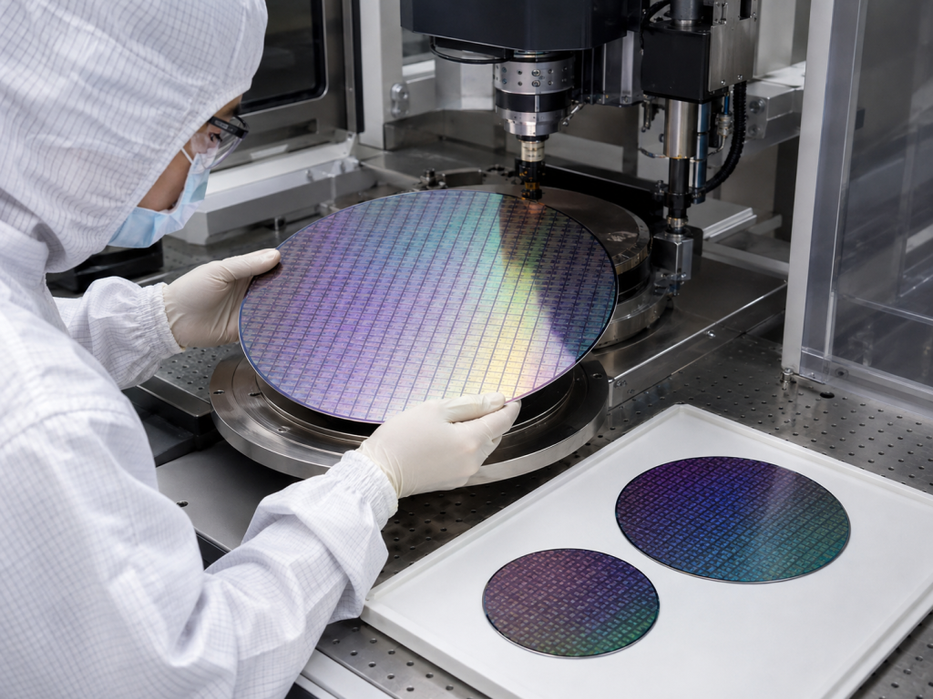
What Is Wafer Resizing?
Wafer resizing is the process of reducing the outer diameter of an existing wafer while preserving as much of its usable surface as possible.
Common resizing projects include:
- Converting a 300mm wafer to 200mm
- Converting a 300mm wafer to 150mm
- Converting a 200mm wafer to 150mm
- Producing custom diameters such as 100mm, 125mm, 180mm or 190mm
- Removing a damaged or contaminated outer edge
- Creating smaller samples from full-size wafers
- Modifying wafer dimensions for legacy semiconductor equipment
- Preparing substrates for custom holders, carriers or bonding fixtures
The source wafer may be made from silicon, glass, fused silica, sapphire, silicon carbide, gallium arsenide, indium phosphide or another brittle substrate material.
The machining method must be selected according to the mechanical properties of the material and the condition of the wafer.
Why Convert a 300mm Wafer to a Smaller Diameter?
A 300mm wafer may contain valuable films, coatings, test structures or device layers, but the next processing step may only be available on a 200mm or 150mm platform.
Typical reasons for resizing include:
Legacy equipment compatibility
Many research and production tools are designed for 100mm, 150mm or 200mm wafers. Resizing allows a larger wafer or coated substrate to be processed using existing equipment without purchasing a new 300mm tool.
Research and process development
Universities, laboratories and semiconductor development teams may only need a smaller section of an expensive wafer. Converting a 300mm wafer into smaller round substrates can reduce material consumption during testing.
Equipment qualification
Custom-size wafers may be used to test wafer handling systems, robots, vacuum chucks, deposition chambers and inspection equipment.
Removal of edge defects
The outer area of a wafer may contain edge chips, coating non-uniformity, contamination or handling damage. Controlled diameter reduction can remove the affected region and preserve the central usable area.
Custom fixture requirements
Some bonding, thinning, polishing and metrology systems use non-standard wafer holders. A resized wafer may be required to match the fixture diameter and clamping structure.
Can Every 300mm Wafer Be Resized?
Not every wafer is equally suitable for resizing. Feasibility should be evaluated before machining.
The following factors are important:
- Wafer material
- Original diameter
- Target diameter
- Wafer thickness
- Surface condition
- Presence of deposited films
- Device or pattern location
- Edge exclusion area
- Existing notch or orientation flat
- Bow and warp
- Frontside protection requirements
- Backside contamination limits
- Acceptable edge chipping
- Final strength requirements
A bare silicon wafer is generally easier to resize than a thin device wafer containing fragile MEMS structures, metal layers or sensitive coatings.
Ultra-thin wafers may require temporary bonding to a rigid carrier before diameter machining. Without sufficient support, the wafer can crack, flex or break under grinding and handling forces.
Typical Wafer Resizing Process
The exact manufacturing route varies, but a controlled resizing project normally includes the following steps.
1. Incoming wafer inspection
Before machining, the wafer should be checked for:
- Existing edge chips
- Surface scratches
- Cracks
- Film delamination
- Bow and warp
- Thickness variation
- Notch or flat position
- Contamination
- Frontside and backside condition
Photographs and inspection records are useful when processing high-value wafers.
2. Surface protection
If the wafer has a polished, coated or patterned front surface, protective film may be applied before machining.
The protection method must be compatible with:
- Surface coating
- Adhesion limitations
- Cleaning chemicals
- Processing temperature
- Particle-control requirements
Sensitive device wafers may require a low-residue protective film or temporary bonding process.
3. Temporary support or carrier bonding
Thin wafers often need mechanical support. The wafer may be temporarily mounted on a glass, silicon or metal carrier using wax, adhesive or another removable bonding material.
Carrier support can help reduce:
- Wafer flexing
- Vibration
- Edge fracture
- Surface damage
- Handling breakage
The bonding and debonding method must not damage existing films or leave unacceptable residue.
4. Diameter cutting or coring
A smaller circular wafer is produced from the larger source wafer. Depending on the material and tolerance requirements, the process may use controlled mechanical coring, precision grinding or another suitable machining method.
The initial cut normally leaves machining allowance for final diameter finishing.
The target circle should be positioned carefully to avoid:
- Important device patterns
- Test structures
- Defective regions
- Existing edge damage
- Non-uniform coatings
5. Outer-diameter grinding
After rough cutting, the outer diameter is precision-ground to the required size.
Important parameters include:
- Target diameter
- Diameter tolerance
- Roundness
- Concentricity
- Edge chipping limit
- Feed rate
- Grinding wheel selection
For brittle materials, aggressive machining can create microcracks that reduce wafer strength.
6. Notch or orientation-flat reconstruction
When the resized wafer must remain compatible with automated equipment, a new notch or orientation flat may be required.
The buyer should specify:
- Notch or flat type
- Angular position
- Orientation reference
- Width and depth
- Dimensional tolerance
- Relationship to crystal orientation or device layout
The original notch cannot usually remain after a large diameter reduction, especially when converting a 300mm wafer to 200mm or 150mm.
7. Edge beveling and rounding
A sharp, vertical edge is vulnerable to chipping and crack propagation. Edge beveling or rounding improves mechanical strength and handling safety.
The edge profile may include:
- Rounded edge
- Symmetrical bevel
- Asymmetrical bevel
- Chamfer
- Custom profile
The selected profile should match the wafer thickness and downstream handling equipment.
8. Cleaning
Machining produces particles, grinding debris and possible adhesive residue. Cleaning is necessary before final inspection and packaging.
Cleaning requirements depend on whether the wafer is:
- A bare substrate
- A coated wafer
- A patterned device wafer
- A dummy wafer
- A research sample
- A production-grade wafer
Some films cannot tolerate aggressive chemical cleaning, ultrasonic cleaning or high-temperature drying. Buyers should disclose all material compatibility restrictions.
9. Final inspection
Final inspection may include:
- Diameter
- Thickness
- Total thickness variation
- Bow
- Warp
- Roundness
- Notch or flat dimensions
- Edge profile
- Edge chipping
- Surface condition
- Particle level
- Visual appearance
For critical applications, dimensional reports and inspection photographs can be supplied with the wafers.
Recommended Specifications for a Resized Wafer
The table below shows typical items that should be defined in an RFQ. Actual tolerances depend on the wafer material, thickness and processing condition.
| Specification | Information to Provide |
|---|---|
| Source wafer diameter | 300mm, 200mm or other |
| Target diameter | 200mm, 150mm or custom |
| Diameter tolerance | Required upper and lower limits |
| Wafer material | Silicon, glass, sapphire, SiC or compound semiconductor |
| Wafer thickness | Nominal thickness and tolerance |
| Surface condition | Polished, coated, patterned or device wafer |
| Frontside protection | Required or not required |
| Orientation feature | Notch, flat or no orientation feature |
| Orientation angle | Position relative to crystal or pattern |
| Edge profile | Rounded, bevelled, chamfered or custom |
| Maximum edge chipping | Acceptable chip width and depth |
| TTV | Maximum allowable total thickness variation |
| Bow and warp | Maximum allowable values |
| Cleaning requirement | Standard cleaning or restricted process |
| Inspection report | Dimensional, visual or metrology report |
| Packaging | Single-wafer box, cassette or custom packaging |
Important Tolerances
Diameter tolerance
The acceptable diameter tolerance depends on the wafer holder and equipment interface. A loose tolerance may be acceptable for manual laboratory use, while automated handling systems may require tighter control.
Roundness
A wafer can meet the average diameter requirement but still be out of round. Roundness should be controlled when the wafer will be rotated, aligned or handled automatically.
TTV, bow and warp
Resizing does not automatically improve wafer flatness. Mechanical stress, carrier bonding and edge processing may affect bow and warp, especially for thin wafers or multilayer structures.
For bonding, lithography and vacuum chuck applications, buyers should define maximum TTV, bow and warp values.
Notch position
The notch may be used for crystal orientation, equipment alignment or pattern registration. Incorrect angular positioning can make the wafer incompatible with downstream tools.
The RFQ should clearly state the reference used to define notch position.
Edge chipping
Small edge chips may be acceptable for test samples but unacceptable for high-speed rotation, automated handling or repeated thermal cycling.
Edge acceptance criteria should include both chip size and chip quantity.
Risks When Resizing Patterned or Device Wafers
Patterned wafers require additional process control because the wafer already contains valuable structures.
Potential risks include:
- Scratching of the device surface
- Metal contamination
- Protective-film residue
- Pattern damage near the new edge
- Cracking caused by internal film stress
- Particle deposition
- Damage during debonding
- Loss of wafer orientation
- Excessive edge exclusion
Before processing, the customer should provide a pattern map showing the usable device area and the proposed target circle.
A larger safety margin should be reserved between the machining path and active structures.
Resizing Thin Wafers
Thin wafers are more difficult to machine because they have lower stiffness and fracture strength.
Special attention is required when processing wafers below approximately 300µm, although the actual handling risk depends on diameter, material and film structure.
Possible control measures include:
- Temporary carrier bonding
- Low-force machining
- Reduced feed rate
- Fine-grit edge finishing
- Controlled debonding
- Low-stress cleaning
- Single-wafer packaging
For ultra-thin wafers, a feasibility test using a sacrificial sample may be recommended before processing valuable device wafers.
Wafer Resizing Versus Wafer Dicing
Wafer resizing and wafer dicing are different operations.
Wafer resizing changes the outer diameter while maintaining a round wafer format. Wafer dicing separates a wafer into individual rectangular or irregular dies.
A resized wafer can still be processed in standard wafer equipment, provided that its diameter, notch and edge profile are compatible with the system.
Wafer resizing is therefore more suitable for:
- Equipment retrofit
- Round substrate preparation
- Legacy-tool compatibility
- Wafer-level bonding
- Deposition experiments
- Custom wafer carriers
- Research-scale processing
Packaging and Transportation
After resizing, the wafer edge may be more sensitive than the original factory-finished edge. Proper packaging is therefore essential.
Recommended packaging options include:
- Individual wafer boxes
- Non-contact edge-support containers
- Cleanroom-compatible cushioning
- Vacuum-sealed moisture-barrier bags
- Custom carriers for thin or fragile wafers
The wafer should not move freely inside the package. For coated or patterned wafers, the active surface must not contact packaging materials.
RFQ Checklist for Wafer Resizing Services
To receive an accurate quotation and feasibility assessment, buyers should provide:
- Source wafer material and diameter
- Target wafer diameter
- Wafer thickness
- Quantity
- Bare, coated or patterned surface condition
- Film or device structure information
- Frontside and backside photographs
- Target circle or pattern map
- Required notch or flat
- Crystal-orientation requirement
- Diameter and roundness tolerance
- Edge profile requirement
- Maximum acceptable edge chipping
- TTV, bow and warp limits
- Cleaning restrictions
- Inspection and reporting requirements
- Packaging requirements
- Final application and equipment type
The more complete the RFQ information, the easier it is to select a safe machining and inspection process.
How to Choose a Wafer Resizing Supplier
A qualified resizing supplier should evaluate the entire wafer structure rather than only the requested diameter.
Important capabilities include:
- Precision wafer coring and outer-diameter grinding
- Experience with brittle semiconductor materials
- Thin-wafer carrier bonding
- Notch and orientation-flat machining
- Edge beveling and polishing
- Surface-protection control
- Clean handling and packaging
- Dimensional inspection
- Small-batch and prototype support
- Processing of customer-supplied wafers
For expensive device wafers, the supplier should confirm process risks before production and establish clear acceptance criteria.
Conclusion
Converting a 300mm wafer into a 200mm, 150mm or custom-diameter wafer can make valuable substrates compatible with legacy equipment, laboratory tools and specialized processing systems.
However, successful resizing requires more than cutting a smaller circle. Diameter tolerance, roundness, notch orientation, edge strength, surface protection, cleaning and final inspection must all be considered.
Buyers should provide complete information about the wafer material, thickness, surface structure, target diameter and downstream application. A clearly defined RFQ helps reduce breakage risk, prevent surface damage and ensure that the resized wafer can be used reliably in the next process.
Frequently Asked Questions
Can a 300mm silicon wafer be resized to 200mm?
Yes. A smaller circular substrate can be machined from the usable area of a 300mm wafer. The final feasibility depends on wafer thickness, surface condition, pattern location and required edge quality.
Can a new notch be added after wafer resizing?
Yes. A new notch or orientation flat can be machined, but its position, size and orientation reference must be specified before processing.
Can patterned device wafers be resized?
Patterned wafers can be resized, but they require surface protection and a clear device-layout map. The machining path must remain outside the active device region.
Does wafer resizing affect TTV, bow or warp?
The resizing process may influence mechanical stress and flatness, particularly for thin or multilayer wafers. Final TTV, bow and warp should be inspected when these parameters are important.
What is the minimum order quantity?
Prototype and small-batch wafer resizing can usually be evaluated, but the minimum quantity depends on wafer material, setup requirements and inspection specifications.
Can custom diameters other than 150mm and 200mm be produced?
Yes. Custom diameters may be possible when the required dimensions, tolerances, edge profile and equipment compatibility are clearly defined.