
1. Introduction
Wafer dicing (also called wafer singulation) is a critical step in semiconductor manufacturing, where processed silicon or compound semiconductor wafers are separated into individual dies. As device geometries shrink and materials diversify—such as silicon carbide (SiC), gallium nitride (GaN), and sapphire—the choice of dicing technology becomes increasingly important.
Two dominant approaches are widely used today:
- Mechanical dicing (diamond blade sawing)
- Laser dicing (laser-based ablation or stealth separation)
Each method has distinct physical mechanisms, process constraints, and application domains. This article provides a scientific comparison of both technologies in terms of principles, performance, and industrial suitability.
2. Fundamental Working Principles
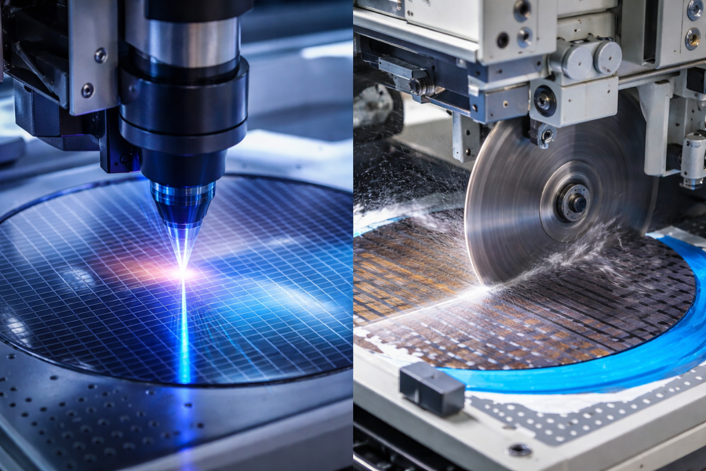
2.1 Mechanical Wafer Dicing (Diamond Sawing)
Mechanical dicing uses a high-speed rotating spindle equipped with a diamond-embedded blade. The wafer is mounted on dicing tape and cut along predefined streets.
The process is governed by material removal through abrasion and fracture mechanics:
- Diamond particles mechanically scratch and fracture the wafer
- Material is removed as fine debris (slurry or dry particles depending on system)
- Cooling water is often used to reduce thermal and mechanical stress
This method is mature and widely adopted in semiconductor fabs.
2.2 Laser Wafer Dicing
Laser dicing uses a highly focused laser beam (nanosecond, picosecond, or femtosecond pulses) to modify or remove material.
Common mechanisms include:
- Laser ablation: direct vaporization of material
- Stealth dicing: subsurface modification followed by controlled fracture
- Thermal stress separation: localized heating induces crack propagation
Unlike mechanical contact cutting, laser dicing is a non-contact process, reducing mechanical stress on the wafer.
3. Process Comparison
3.1 Mechanical Stress and Damage
Mechanical dicing introduces:
- Edge chipping
- Microcracks
- Stress propagation in brittle materials
Laser dicing reduces mechanical force, but may introduce:
- Heat-affected zones (HAZ)
- Microstructural modification depending on wavelength and pulse duration
For brittle and high-value materials (e.g., SiC wafers), damage control is critical.
3.2 Precision and Kerf Width
- Mechanical saw kerf: typically 25–60 µm (depends on blade thickness)
- Laser kerf: can be reduced to <20 µm in optimized systems
Laser technology provides higher flexibility for ultra-fine geometries, especially in advanced packaging and MEMS devices.
3.3 Material Compatibility
| Material Type | Mechanical Saw | Laser Dicing |
|---|---|---|
| Silicon (Si) | Widely used | Increasing use |
| SiC | Difficult (tool wear) | Preferred (advanced systems) |
| Sapphire | High chipping risk | Better edge quality |
| GaN | Moderate damage | Preferred |
Laser dicing becomes increasingly advantageous for hard, brittle, and wide bandgap materials.
3.4 Throughput and Cost Efficiency
Mechanical dicing:
- High throughput
- Lower equipment cost
- Mature consumables ecosystem (blades, coolant)
Laser dicing:
- Higher capital investment
- Lower consumable cost
- Potentially slower in some configurations (depending on scan strategy)
In high-volume silicon manufacturing, mechanical sawing still dominates due to cost efficiency.
3.5 Tool Wear and Maintenance
Mechanical systems suffer from:
- Blade wear
- Frequent replacement
- Process drift over time
Laser systems:
- No physical tool wear
- Requires optical alignment and lens maintenance only
This makes laser systems attractive for long-term stability in precision manufacturing.
4. Industrial Applications
4.1 Mechanical Dicing Applications
- CMOS image sensors
- Memory chips (DRAM, NAND)
- Standard silicon IC packaging
4.2 Laser Dicing Applications
- SiC power devices (EV, charging infrastructure)
- LED and optoelectronic wafers
- MEMS devices
- Advanced heterogeneous integration packaging
5. Key Trade-Off Summary
From an engineering perspective, the choice between laser and mechanical dicing depends on balancing:
- Yield vs cost
- Material hardness vs throughput
- Precision vs scalability
Mechanical dicing remains the backbone of mainstream semiconductor production, while laser dicing is rapidly expanding in advanced materials and high-value applications.
6. Future Development Trends
Several trends are shaping the evolution of wafer singulation:
6.1 Hybrid Dicing Systems
Some manufacturers are combining:
- Laser pre-scribing + mechanical breaking
- Laser grooving + blade finishing
This improves both yield and throughput.
6.2 Ultra-Short Pulse Lasers
Femtosecond laser systems significantly reduce heat-affected zones, enabling:
- Cleaner edges
- Reduced microcracks
- Improved reliability in SiC and sapphire wafers
6.3 300mm Wafer Challenges
As wafer size increases:
- Mechanical stress distribution becomes more complex
- Warpage control is critical
- Laser precision becomes more valuable
7. Conclusion
Laser dicing and mechanical sawing represent two fundamentally different engineering approaches to wafer singulation.
- Mechanical saws excel in cost efficiency and high-volume silicon production
- Laser dicing excels in precision, material flexibility, and advanced semiconductor applications
Rather than replacing each other completely, these technologies are increasingly coexisting in a complementary manufacturing ecosystem, driven by material innovation and device miniaturization.