
1. Introduction
With the rapid development of electric vehicles, renewable energy, 5G communication, and high-performance computing, traditional silicon-based semiconductors are increasingly limited in high-power, high-frequency, and high-temperature environments. Silicon carbide (SiC) and gallium nitride (GaN), as wide-bandgap semiconductor materials, offer high breakdown voltage, excellent thermal conductivity, and superior high-frequency performance, making them core materials for next-generation semiconductor devices.
Alongside material advancements, semiconductor processing equipment is evolving to meet the challenges of these new materials. This article provides a scientific overview of equipment trends, key features, and future directions in next-generation semiconductor processing.
2. SiC Wafer Processing Equipment
SiC wafers are extremely hard, thermally conductive, and brittle, imposing high demands on processing equipment. Typical equipment for SiC wafer fabrication includes:
- High-Temperature High-Pressure (PVT) Furnaces – for growing high-quality single-crystal SiC ingots.
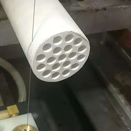
- Precision Wire Saws – utilizing diamond wire or laser cutting to ensure wafer thickness and dimensional accuracy.
- Chemical Mechanical Polishing (CMP) Equipment – for planarizing wafer surfaces, minimizing defects and surface roughness.
- Laser Etching and Marking Systems – for microfabrication in power devices and optoelectronic applications.
As SiC devices move toward larger wafer diameters (e.g., 200mm and 300mm), high-precision cutting, polishing, and automated wafer handling systems become industry priorities.
3. GaN Semiconductor Processing Equipment
Gallium nitride (GaN) is primarily used in high-frequency RF devices and power electronics. GaN wafers are often grown on silicon or sapphire substrates, so processing equipment must accommodate heterogeneous substrates:
- MOCVD (Metal-Organic Chemical Vapor Deposition) Systems – the core equipment for GaN thin-film growth, controlling thickness and doping accuracy.
- ICP Dry Etchers – for microstructure patterning with high aspect ratios and smooth sidewalls.
- Automated Wafer Handling Systems – reducing breakage and improving yield for fragile GaN wafers.
GaN equipment trends focus on small-batch high-precision fabrication, low defect rates, and multi-substrate compatibility to meet the needs of 5G base stations and fast-charging electric vehicle applications.
4. Composite Materials and Next-Generation Equipment
Beyond SiC and GaN, composite semiconductor materials (e.g., SiC/GaN hybrid devices, multi-layer heterostructures) are emerging. Composite materials introduce new challenges for equipment:
- Multi-material Compatibility – equipment must process materials with different hardness and thermal expansion coefficients in the same workflow.
- High-Precision Alignment and Packaging – nanoscale alignment is critical for heterogeneous integration.
- Advanced Monitoring and Control – online inspection, AI visual recognition, and temperature control ensure process stability.
These demands are driving equipment development toward modular, intelligent, and composite-material-compatible designs.
5. Automation and Smart Equipment
Future semiconductor equipment development emphasizes automation and intelligence:
- Industrial 4.0 Integration – real-time monitoring of wafers and processing parameters enables data-driven optimization.
- AI-Assisted Control – machine learning optimizes cutting paths, polishing pressures, and deposition parameters, improving yield.
- Robotic Handling Systems – reduce manual intervention, enhance safety, and ensure repeatability, especially for fragile SiC and GaN wafers.
Smart equipment will become standard in high-end semiconductor fabrication, balancing productivity, precision, and cost.
6. Application Outlook
- Electric Vehicles and Renewable Energy – SiC power devices significantly reduce energy loss and improve inverter efficiency.
- 5G and RF Communications – GaN devices excel in high-frequency, high-power applications.
- High-Performance Computing and Optoelectronics – composite materials enable miniaturization and high integration of chips.
As demand grows, processing equipment will continue to evolve, offering high-precision, low-defect, and intelligent customized solutions.
7. Conclusion
Next-generation semiconductor processing equipment is evolving around SiC, GaN, and composite materials. Key development trends include:
- High-precision cutting and polishing
- Compatibility with heterogeneous and composite materials
- Smart automation and AI-assisted control
Investing in advanced processing equipment allows semiconductor manufacturers to maximize the performance advantages of new materials, supporting the development of higher-power, higher-frequency, and more reliable devices. By keeping pace with these technological trends, the industry can accelerate innovation in electric vehicles, 5G communication, high-performance computing, and other emerging applications. Companies like ZMSH provide customized processing solutions to help manufacturers optimize SiC and GaN wafer production efficiently.