
Silicon wafers are normally supplied in standardized diameters, but semiconductor R&D, MEMS, sensor development, university research, legacy equipment, and specialized fabrication processes often require substrates smaller than the original wafer.
A typical requirement may involve converting:
- 300 mm silicon wafers to 200 mm;
- 300 mm wafers to 150 mm;
- 200 mm wafers to 100 mm;
- standard wafers to non-standard circular diameters;
- large wafers into several smaller research substrates.
In these applications, silicon wafer coring can be used to extract a smaller circular wafer from a larger source wafer.
However, successful wafer resizing involves much more than simply producing the correct diameter. The newly created wafer must also be evaluated for edge condition, thickness variation, bow, warp, surface damage, cleanliness, and dimensional accuracy before it is used in downstream semiconductor equipment.
This guide explains the major engineering considerations involved in silicon wafer coring and post-coring inspection.
What Is Silicon Wafer Coring?
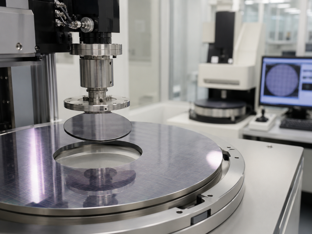
Silicon wafer coring is a precision machining process used to create a smaller circular substrate from a larger silicon wafer.
For example, a 150 mm circular wafer may be extracted from a 200 mm or 300 mm wafer while retaining the original polished surface, deposited layer, crystal orientation, or other valuable wafer characteristics.
Unlike conventional wafer dicing, which mainly follows straight cutting paths to create dies or rectangular samples, coring is designed specifically for circular diameter reduction.
Các ứng dụng điển hình bao gồm:
- wafer resizing;
- legacy equipment compatibility;
- custom semiconductor substrates;
- R&D wafer preparation;
- bonded wafer resizing;
- thin-film substrate conversion;
- MEMS development;
- university research;
- material characterization;
- optical and sensor applications.
For high-value wafers, coring can also allow useful regions of a larger substrate to be recovered rather than purchasing a new wafer in another diameter.
Common Silicon Wafer Diameter Reduction Projects
Typical resizing projects include:
300 mm to 200 mm
This is one of the most practical diameter-conversion cases.
A 300 mm wafer may contain a specialized surface layer, bonded structure, deposited film, or experimental material that must be processed on equipment designed for 200 mm wafers.
300 mm to 150 mm
This conversion is frequently useful for R&D systems and older processing tools.
Because a 150 mm wafer occupies significantly less area than the original 300 mm substrate, remaining material may potentially be used for additional samples depending on the project layout.
200 mm to 100 mm
Research facilities may use 100 mm equipment even when the starting material is commercially available only as a 150 mm or 200 mm wafer.
Custom Diameter Conversion
Some laboratory equipment, vacuum fixtures, optical systems, deposition systems, and custom process chambers require non-standard wafer diameters.
Examples might include:
- 75 mm;
- 80 mm;
- 125 mm;
- 180 mm;
- other customer-specified diameters.
In these projects, the final tolerance and edge geometry should be specified before machining.
Why Diameter Alone Is Not Enough
A wafer can meet its nominal diameter and still be unsuitable for downstream use.
The resizing process may influence:
- edge chipping;
- edge cracks;
- local mechanical stress;
- particle generation;
- wafer flatness;
- bow;
- warp;
- surface cleanliness;
- coating integrity;
- notch orientation.
This is why a finished wafer should normally be evaluated as a precision substrate, not simply as a circular piece of silicon.
Edge defects are especially important because chipping can reduce mechanical strength and contribute to breakage during later handling or processing. DISCO notes that wafer-edge chipping can adversely affect wafer strength and that optimized grinding or edge processing can reduce this damage.
Silicon Wafer Coring Process Flow
A typical coring project may include the following stages.
1. Incoming Wafer Inspection
Before machining, the source wafer should be reviewed for:
- original diameter;
- thickness;
- polished side;
- crystal orientation;
- notch or flat position;
- visible defects;
- coatings;
- patterned areas;
- bonded layers;
- usable region.
For processed wafers, a drawing or map identifying the region that must be preserved can be especially useful.
2. Coring Position Definition
The required circular region is positioned within the original wafer.
For a simple blank wafer, the smaller diameter may normally be centered.
For patterned or deposited wafers, however, the desired region may need to be intentionally offset to preserve:
- a device area;
- deposited film;
- epitaxial region;
- bonded structure;
- test pattern.
3. Circular Cutting
A precision circular machining process separates the desired wafer from the surrounding material.
Processing parameters must be selected according to:
- silicon thickness;
- wafer diameter;
- cutting tool;
- mounting method;
- surface condition;
- film structure;
- required edge quality.
4. Diameter Finishing
The initial cut may be followed by precision edge grinding or dimensional finishing to bring the wafer to the requested diameter tolerance.
5. Edge Profiling
Depending on the application, the newly created edge may require:
- chamfering;
- beveling;
- rounding;
- edge grinding;
- edge polishing.
6. Cleaning
Machining debris and particles should be removed before final inspection or packaging.
7. Final Metrology
Possible measurements include:
- diameter;
- thickness;
- TTV;
- bow;
- warp;
- notch dimensions;
- edge condition;
- surface condition.
Why Edge Profile Matters After Coring
A standard prime silicon wafer does not normally have a completely sharp 90-degree edge.
Its edge geometry is engineered to improve handling reliability and mechanical robustness.
After a larger wafer is cored, the newly generated edge does not automatically reproduce the original wafer’s edge profile.
If the new edge remains too sharp or contains significant chips, the wafer may become more vulnerable to:
- cracking;
- edge breakage;
- particle generation;
- handling damage;
- failure during subsequent grinding or thermal processing.
DISCO describes edge trimming as a method for reducing wide edge chipping and preventing sharp edge geometry during wafer thinning processes, illustrating why edge geometry is important to wafer mechanical reliability.
For demanding semiconductor applications, the RFQ should therefore specify whether the customer requires:
As-cut edge
hoặc
Ground / chamfered / rounded finished edge
These are not equivalent conditions.
Edge Chipping Inspection
After coring, the edge should be examined for visible machining damage.
Possible defects include:
- large chips;
- micro-chipping;
- radial cracks;
- edge fractures;
- delamination of surface films;
- localized breakage.
Mechanical wafer processing can generate chipping, and tool condition and processing parameters can influence the resulting cut quality. DISCO notes that deterioration of blade shape can contribute to kerf changes and sporadic chipping in wafer cutting applications.
For sensitive projects, customers may want to define acceptable maximum edge-chip dimensions before processing.
What Is TTV?
TTV means Total Thickness Variation.
It describes the difference between the maximum and minimum measured wafer thickness across the evaluated area.
In simplified form:
TTV = Độ dày tối đa − Độ dày tối thiểu
TTV is commonly expressed in micrometers.
SEMI documentation treats thickness, TTV, bow and warp as distinct wafer geometry parameters and provides standardized approaches for their measurement.
A lower TTV generally indicates more uniform wafer thickness.
Does Coring Change TTV?
Coring itself primarily changes wafer diameter rather than intentionally changing wafer thickness.
Therefore, if a source wafer already has good thickness uniformity and the coring operation does not include surface grinding, the center-area thickness distribution may remain largely related to the original wafer.
However, the measured TTV of the newly created wafer can differ from the value reported for the original large wafer because the measurement area has changed.
Ví dụ:
A 300 mm wafer may have one thickness distribution across its full surface, while a 100 mm wafer extracted from one particular region represents only a subset of that original geometry.
Therefore, customers with strict thickness requirements should specify:
- final thickness;
- final TTV;
- measurement method;
- measurement area.
Do not assume the original wafer certificate automatically represents the geometry of the resized wafer.
Wafer Bow là gì?
Wafer bow describes the overall curvature of a free, unclamped wafer relative to a reference plane.
SEMI terminology defines bow using the displacement of the wafer’s median surface around the center region relative to a reference plane.
Bow can result from factors such as:
- residual stress;
- deposited-film stress;
- bonded-layer stress;
- thermal processing;
- wafer thinning;
- material structure.
The importance of bow depends heavily on the downstream application.
“Wafer Warp” là gì?
Warp describes the overall deviation of the wafer surface or median plane from a reference condition, considering both maximum and minimum deviations.
SEMI measurement guidance treats warp separately from bow because the two parameters describe different aspects of wafer shape.
A wafer can therefore have acceptable bow but still show significant non-uniform shape across the surface.
For applications such as:
- lithography;
- wafer bonding;
- advanced packaging;
- precision chucking;
- automated handling;
wafer geometry can become an important process-control parameter. KLA, for example, provides wafer-geometry metrology systems specifically for monitoring wafer shape, stress and warp in semiconductor manufacturing.
Can Coring Affect Bow and Warp?
The answer depends on the wafer structure.
For a relatively thick, bare silicon wafer with low residual stress, diameter reduction may have limited influence on global shape.
However, the situation can be different for:
- very thin wafers;
- oxide-coated wafers;
- metal-coated wafers;
- epitaxial wafers;
- bonded wafers;
- SOI wafers;
- wafers with stressed films;
- partially processed device wafers.
When material is removed around the perimeter, the balance of mechanical stresses can change.
For this reason, bow and warp should be re-measured after coring when wafer shape is important to downstream processing.
Special Considerations for Thin Silicon Wafers
Thin wafers require more careful handling than standard-thickness substrates.
Potential risks include:
- wafer flexing;
- breakage;
- edge cracking;
- handling damage;
- mounting distortion.
Mechanical processing of thin wafers requires specialized control because wafer strength and edge condition become increasingly important as thickness is reduced. DISCO’s wafer-processing guidance highlights edge chipping and wafer-thinning considerations as key challenges in ultra-thin wafer processing.
When requesting coring of a thin wafer, provide the exact thickness rather than simply describing it as “thin.”
Coring Process for Coated or Patterned Wafers
Coring a bare silicon wafer is usually simpler than processing a wafer containing functional films or devices.
Customers should identify any:
- SiO₂ layers;
- SiN layers;
- metals;
- photoresist;
- polymers;
- epitaxial layers;
- bonded layers;
- MEMS structures;
- device patterns.
Possible risks include:
- film cracking;
- delamination;
- contamination;
- scratches;
- water exposure;
- particle deposition.
For processed wafers, it is useful to define a keep-out zone around the new wafer edge.
This reduces the risk that active features will be located too close to the machining region.
Notch and Orientation Requirements
When a 300 mm or 200 mm wafer is reduced to a smaller diameter, the original notch may be removed.
If the resized wafer will be used in equipment that depends on orientation referencing, a new notch or flat may need to be machined.
The customer should provide:
- crystal orientation;
- desired notch direction;
- notch dimensions;
- angular tolerance;
- flat requirement if applicable.
For research projects where orientation is not critical, a new notch may not always be necessary.
For semiconductor processing, however, this should be determined before machining.
Recommended Post-Coring Inspection
A useful final inspection sequence can include the following.
1. Diameter Measurement
Confirm:
- target diameter;
- diameter tolerance;
- roundness where required.
2. Thickness Measurement
Verify the final substrate thickness.
3. TTV Measurement
Confirm thickness uniformity across the newly resized wafer.
4. Bow Measurement
Evaluate the global curvature of the free wafer.
5. Warp Measurement
Check overall wafer shape across the substrate.
6. Edge Inspection
Inspect for:
- chips;
- cracks;
- sharp sections;
- incomplete grinding;
- abnormal edge damage.
7. Surface Inspection
Check the polished surface for:
- scratches;
- handling marks;
- particles;
- contamination;
- coating damage.
8. Notch Inspection
Where applicable, confirm:
- orientation;
- position;
- geometry.
9. Cleaning Verification
For semiconductor applications, the wafer should be processed and packaged according to the cleanliness requirements agreed for the project.
Example: 300 mm to 200 mm Silicon Wafer Coring
Consider the following project:
Starting wafer
- Material: Silicon
- Diameter: 300 mm
- Thickness: 775 µm
- Surface: DSP
- Condition: Bare silicon
Required output
- Diameter: 200 mm
- Circular wafer
- Controlled edge profile
- New orientation reference
- Final dimensional inspection
A possible process flow would be:
Incoming inspection
↓
Coring layout
↓
Circular wafer cutting
↓
Diameter finishing
↓
Edge grinding / chamfering
↓
Notch processing
↓
Vệ sinh
↓
Diameter and thickness inspection
↓
TTV / bow / warp measurement
↓
Edge and surface inspection
↓
Bao bì
The exact sequence should be adjusted according to the customer’s material and tolerance requirements.
Example: 300 mm to 150 mm Processed Wafer
A more difficult case may involve:
- 300 mm silicon wafer;
- deposited thin film;
- patterned center region;
- customer requires a 150 mm circular sample.
Before processing, additional information is necessary:
- Which region must be preserved?
- Is the film sensitive to water?
- Is the wafer front side protected?
- How close may machining approach the active area?
- Is the film under significant stress?
- Does final bow matter?
- Is a new notch required?
In this situation, coring should be treated as a customized substrate-processing project rather than ordinary mechanical cutting.
Coring Multiple Small Wafers from One Large Wafer
Another option is extracting several smaller circular wafers from a larger substrate.
Whether this is practical depends mainly on:
- original diameter;
- required final diameter;
- spacing between cuts;
- edge allowance;
- notch location;
- usable wafer area;
- surface defects;
- desired orientation.
For expensive experimental wafers, optimizing the cutting layout can improve material utilization.
Any remaining usable regions can also potentially be diced into rectangular research coupons.
What Information Should Be Included in a Silicon Wafer Coring RFQ?
For faster technical evaluation and quotation, provide the following information:
Starting Wafer
- material;
- diameter;
- thickness;
- crystal orientation;
- doping type;
- polished side;
- notch or flat;
- bare or processed condition.
Required Finished Wafer
- target diameter;
- diameter tolerance;
- thickness;
- TTV;
- bow;
- warp;
- notch or flat;
- edge profile.
Surface Information
Indicate whether the wafer contains:
- oxide;
- nitride;
- metal;
- epitaxy;
- bonded layers;
- device patterns;
- photoresist;
- sensitive coatings.
Inspection Requirements
Specify whether you require:
- dimensional report;
- TTV measurement;
- bow measurement;
- warp measurement;
- microscope edge inspection;
- surface inspection;
- photographs.
Số lượng
State both:
- number of source wafers;
- number of finished wafers required.
Common Mistakes When Ordering Wafer Coring
Mistake 1: Specifying Only the Final Diameter
“Please convert 300 mm to 200 mm” is not a complete specification.
Edge profile, notch orientation, tolerance and inspection requirements may be equally important.
Mistake 2: Ignoring the New Edge
The original wafer edge may have been professionally finished, but the newly cored edge is a completely new machined surface.
Its quality must be evaluated separately.
Mistake 3: Using Original TTV Data as Final TTV Data
After resizing, the measurement area changes.
If TTV is critical, measure the finished wafer.
Mistake 4: Ignoring Bow and Warp on Coated Wafers
Film stress can significantly influence wafer geometry.
Always provide information about deposited or bonded structures.
Mistake 5: Forgetting Orientation
If the original notch is removed during diameter reduction, a new orientation reference may be required.
How to Choose a Silicon Wafer Coring Supplier
For semiconductor and research applications, evaluate more than whether a supplier can physically cut silicon.
Important capabilities include:
- precision diameter control;
- edge finishing;
- thin-wafer handling;
- processed-wafer protection;
- custom notch machining;
- cleaning;
- dimensional inspection;
- TTV measurement;
- bow and warp measurement;
- packaging and traceability.
A supplier should also be willing to evaluate unusual wafer structures before promising a finished specification.
Kết luận
Silicon wafer coring is an effective method for converting large-diameter wafers into smaller circular substrates, including 300 mm to 200 mm, 300 mm to 150 mm, 200 mm to 100 mm, and custom-diameter wafers.
But diameter conversion is only one part of a successful resizing project.
The final wafer may also need controlled:
- edge profile;
- edge chipping;
- diameter tolerance;
- thickness;
- TTV;
- bow;
- warp;
- notch orientation;
- surface cleanliness.
For simple bare silicon wafers, the process can be relatively straightforward.
For thin, coated, bonded or device-processed wafers, coring should be evaluated as a complete precision-processing workflow that includes machining, cleaning and post-coring metrology.
When requesting a quotation, provide the original wafer specifications, required final diameter, edge requirements, wafer condition, TTV, bow, warp, notch orientation and inspection criteria. A complete RFQ makes it much easier to determine whether the desired resized wafer can meet the requirements of the next semiconductor process.