
In semiconductor manufacturing, wafer processing depends not only on advanced equipment and high-purity wafers, but also on a wide range of consumable components used inside process chambers, cleaning systems, thermal furnaces, and wafer handling environments. These consumables may appear as supporting parts, shielding parts, carriers, rings, boats, trays, nozzles, tubes, plates, or liners. However, their material performance directly affects process stability, particle control, contamination level, wafer yield, and equipment lifetime.
Semiconductor wafer consumables are exposed to harsh process conditions, including plasma bombardment, corrosive gases, high-purity chemicals, rapid temperature changes, vacuum environments, and high-temperature thermal cycles. As a result, the materials used for these parts must meet strict requirements for purity, corrosion resistance, thermal stability, mechanical strength, dimensional accuracy, and low particle generation.
Common materials used in semiconductor wafer consumables include quartz glass, silicon carbide, alumina ceramics, silicon, graphite, sapphire, boron nitride, and advanced ceramic coatings. Each material has its own advantages and limitations. Understanding these materials helps engineers, buyers, and equipment users select suitable consumables for etching, cleaning, oxidation, diffusion, CVD, PVD, annealing, and other semiconductor processes.
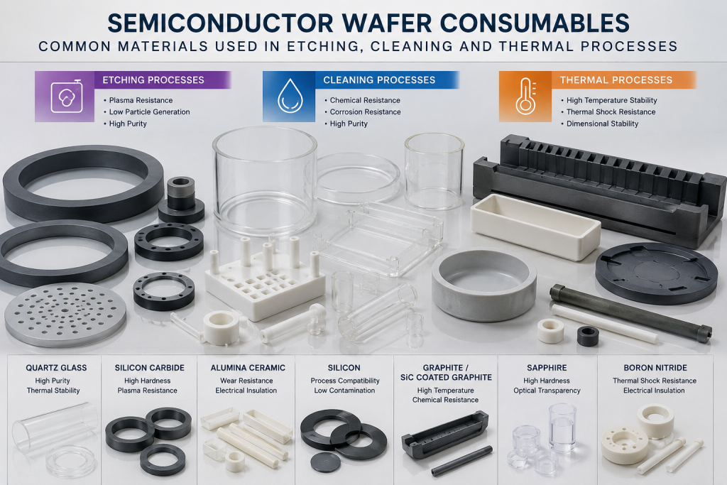
1. What Are Semiconductor Wafer Consumables?
Semiconductor wafer consumables refer to replaceable or regularly maintained components used during wafer fabrication and processing. Unlike permanent equipment structures, consumables are expected to wear, degrade, or become contaminated over time and need replacement after a certain service period.
Typical semiconductor wafer consumables include:
- Wafer boats
- Wafer carriers
- Etching rings
- Focus rings
- Edge rings
- Shield rings
- Susceptors
- Trays
- Process tubes
- Quartz liners
- Gas nozzles
- Cleaning baskets
- Wafer holders
- Ceramic plates
- Insulation parts
- Chamber shields
- Diffusion furnace parts
- CVD and PECVD chamber components
Although these parts may not be active electronic components, their quality can strongly influence the final wafer process result. A poorly selected consumable may introduce particles, metallic contamination, thermal deformation, plasma instability, or chemical corrosion. Therefore, consumable material selection is an important part of semiconductor process engineering.
2. Key Requirements for Wafer Consumable Materials
Different semiconductor processes require different material properties. However, most wafer consumables share several critical requirements.
2.1 High Purity
Semiconductor processes are extremely sensitive to contamination. Metallic impurities such as sodium, iron, copper, nickel, calcium, or potassium may affect device performance. For this reason, consumable materials must have high chemical purity and low impurity release.
2.2 Low Particle Generation
Particles are one of the major causes of defects in wafer fabrication. Consumables must resist abrasion, plasma erosion, cracking, and surface peeling. Smooth surface finish and stable microstructure are important for reducing particle generation.
2.3 Chemical Resistance
Etching and cleaning processes may involve fluorine-based gases, chlorine-based gases, oxygen plasma, strong acids, strong alkalis, or high-purity solvents. Consumable materials must resist corrosion under specific chemical environments.
2.4 Thermal Stability
Thermal processes such as diffusion, oxidation, annealing, and LPCVD require materials that can maintain shape and strength at elevated temperatures. Low thermal expansion, high softening point, and resistance to thermal shock are important.
2.5 Dimensional Accuracy
Wafer processing often requires precise positioning. Consumables such as wafer carriers, trays, and rings must maintain tight tolerances to ensure stable wafer placement, uniform gas flow, and process repeatability.
2.6 Plasma Resistance
In plasma etching and deposition systems, chamber consumables are exposed to ion bombardment and reactive plasma species. Materials must resist erosion while minimizing contamination and particle formation.
3. Quartz Glass Consumables
Quartz glass is one of the most widely used materials in semiconductor wafer processing. It is commonly used in high-temperature furnaces, cleaning systems, diffusion equipment, oxidation processes, and wafer handling environments.
3.1 Typical Quartz Consumables
Quartz consumables include:
- Quartz wafer boats
- Quartz process tubes
- Quartz liners
- Quartz rings
- Quartz flanges
- Quartz trays
- Quartz rods
- Quartz nozzles
- Quartz cleaning tanks
- Quartz beakers
- Quartz carriers
3.2 Advantages of Quartz
Quartz glass offers excellent thermal resistance, chemical stability, optical transparency, and high purity. It is suitable for many high-temperature and chemical processing environments. Its low thermal expansion helps reduce thermal stress during heating and cooling.
Quartz is especially common in diffusion and oxidation furnace systems because it can withstand high temperatures while maintaining good cleanliness.
3.3 Limitations of Quartz
Although quartz has excellent purity and thermal performance, it may soften at very high temperatures and can be attacked by certain fluorine-containing chemistries. Quartz is also brittle, so careful handling and precision fabrication are required.
4. Silicon Carbide Consumables
Silicon carbide is widely used in semiconductor processes that require high temperature resistance, plasma resistance, and strong mechanical performance. It is commonly used in etching chambers, high-temperature carriers, and advanced process environments.
4.1 Typical SiC Consumables
Silicon carbide consumables include:
- SiC focus rings
- SiC edge rings
- SiC shield rings
- SiC trays
- SiC susceptors
- SiC wafer carriers
- SiC boats
- SiC liners
- SiC nozzles
- SiC coated graphite parts
4.2 Advantages of Silicon Carbide
Silicon carbide provides high hardness, excellent wear resistance, high thermal conductivity, strong thermal shock resistance, and good plasma resistance. Compared with quartz, SiC can perform better in more aggressive plasma and high-temperature environments.
In plasma etching equipment, SiC rings and chamber components help improve process stability and reduce contamination. In thermal systems, SiC carriers and trays can support wafers under high-temperature conditions with good dimensional stability.
4.3 Types of SiC Materials
Several forms of silicon carbide are used in semiconductor consumables:
- Sinterlenmiş SiC
- Reaction-bonded SiC
- CVD SiC
- CVD SiC-coated graphite
- Recrystallized SiC
CVD SiC is especially valued for high-purity applications because of its dense structure and excellent surface quality. SiC-coated graphite is often used when a lightweight graphite core is needed together with a chemically stable SiC surface.
5. Alumina Ceramic Consumables
Alumina ceramic is another important material used in semiconductor equipment and wafer processing systems. It is widely selected for insulation, mechanical support, wear resistance, and chemical stability.
5.1 Typical Alumina Consumables
Alumina ceramic consumables include:
- Ceramic plates
- Insulating rings
- Wafer support parts
- Cleaning fixtures
- Ceramic nozzles
- Ceramic pins
- Ceramic guides
- Ceramic arms
- Chamber insulation parts
5.2 Advantages of Alumina
Alumina has good electrical insulation, high hardness, wear resistance, and thermal stability. It is also cost-effective compared with many advanced ceramics. High-purity alumina can be used in process environments where low contamination is required.
5.3 Limitations of Alumina
Alumina may not be suitable for all plasma environments, especially when extremely low particle generation or strong fluorine plasma resistance is required. Its thermal conductivity is lower than that of silicon carbide, and material grade selection is important for semiconductor use.
6. Silicon Consumables
High-purity silicon parts are commonly used in plasma etching systems, especially where material compatibility with silicon wafers is important.
6.1 Typical Silicon Consumables
Silicon consumables include:
- Silicon focus rings
- Silicon edge rings
- Silicon electrodes
- Silicon showerheads
- Silicon plates
- Silicon chamber parts
6.2 Advantages of Silicon
Because silicon is the base material of most semiconductor wafers, silicon consumables can reduce the risk of introducing foreign material contamination. In silicon wafer etching processes, silicon parts may provide excellent compatibility with the process environment.
6.3 Limitations of Silicon
Silicon has lower mechanical toughness compared with some ceramics. It may also erode in plasma environments and requires periodic replacement. High-purity silicon components usually require precision machining and careful surface control.
7. Graphite and SiC-Coated Graphite Consumables
Graphite is used in high-temperature semiconductor processes because of its excellent thermal stability, machinability, and lightweight structure. However, bare graphite may generate particles or release contamination, so it is often coated with CVD SiC or other protective coatings.
7.1 Typical Graphite-Based Consumables
Graphite and SiC-coated graphite components include:
- Susceptors
- Heating elements
- Carriers
- Trays
- Furnace fixtures
- Epitaxy process parts
- CVD support parts
7.2 Advantages
Graphite has excellent high-temperature performance and can be machined into complex shapes. When coated with CVD SiC, the surface becomes more chemically stable, denser, and cleaner for semiconductor use.
7.3 Limitations
The coating quality is critical. If the coating has pinholes, cracks, or poor adhesion, the graphite substrate may become exposed. This can lead to particle contamination or reduced service life.
8. Sapphire Consumables
Sapphire is a single-crystal aluminum oxide material with excellent hardness, optical transparency, chemical resistance, and temperature stability. It is used in special semiconductor and optical process environments.
8.1 Typical Sapphire Components
Sapphire consumables and precision parts include:
- Sapphire windows
- Sapphire tubes
- Sapphire rods
- Sapphire nozzles
- Sapphire pins
- Sapphire optical components
- Sapphire insulating parts
8.2 Advantages of Sapphire
Sapphire provides excellent scratch resistance, high-temperature stability, and optical transmission. It is especially useful in observation windows, optical monitoring systems, plasma equipment, and high-wear environments.
8.3 Limitations
Sapphire is hard and difficult to machine. It is generally more expensive than quartz or alumina. For complex shapes, machining cost and lead time may be higher.
9. Boron Nitride Consumables
Boron nitride is used in semiconductor and high-temperature applications where electrical insulation, thermal stability, and non-wetting behavior are required.
9.1 Typical BN Consumables
Boron nitride components include:
- Insulation parts
- Furnace fixtures
- Crucible components
- Wafer support parts
- High-temperature spacers
- Ceramic liners
9.2 Advantages
Boron nitride has good thermal shock resistance, electrical insulation, and machinability. It is suitable for certain high-temperature and vacuum environments.
9.3 Limitations
BN is relatively soft compared with alumina or SiC. Its suitability depends strongly on the chemical environment, temperature, and mechanical load.
10. Materials Used in Etching Processes
Etching processes are among the most demanding environments for wafer consumables. Plasma, reactive gases, ion bombardment, and chamber by-products can rapidly wear process components.
Common materials used in etching consumables include:
| Malzeme | Typical Etching Application |
|---|---|
| Silisyum karbür | Focus rings, edge rings, chamber liners |
| Silikon | Focus rings, electrodes, showerheads |
| Kuvars | Rings, liners, windows, insulation parts |
| Alumina | Insulators, support parts |
| Safir | Windows, wear-resistant parts |
| Yttria-coated ceramics | Plasma-resistant chamber parts |
For plasma etching, material erosion rate and contamination behavior are key selection factors. The best material depends on gas chemistry, plasma power, wafer type, process temperature, and required lifetime.
11. Materials Used in Cleaning Processes
Wet cleaning systems use high-purity chemicals to remove particles, organic residues, metal ions, and native oxides. Consumables in these environments must resist corrosion and avoid contaminating the wafer.
Common materials used in cleaning consumables include:
| Malzeme | Typical Cleaning Application |
| Kuvars | Tanks, carriers, beakers, wafer holders |
| High-purity ceramics | Fixtures and support parts |
| PTFE/PFA | Chemical tubing and containers |
| Safir | Special nozzles and wear-resistant parts |
| Silisyum karbür | High-durability fixtures in selected processes |
Quartz is widely used because of its purity and chemical stability. However, the choice of material must be matched with the specific acid, alkali, solvent, or cleaning temperature.
12. Materials Used in Thermal Processes
Thermal processes include oxidation, diffusion, annealing, LPCVD, epitaxy, and high-temperature treatment. Consumables in these systems must maintain dimensional stability and cleanliness at high temperatures.
Common thermal process materials include:
| Malzeme | Typical Thermal Application |
| Kuvars | Furnace tubes, boats, liners |
| Silisyum karbür | Boats, trays, carriers, susceptors |
| Graphite | High-temperature support structures |
| SiC-coated graphite | Epitaxy susceptors and carriers |
| Alumina | Insulators and support parts |
| Boron nitride | High-temperature insulation components |
In thermal systems, thermal expansion, temperature uniformity, contamination level, and mechanical strength must be considered together.
13. How to Select the Right Consumable Material
Selecting the right semiconductor wafer consumable material requires understanding both the process environment and the function of the component.
Important selection questions include:
- Is the process dry, wet, plasma-based, or thermal?
- What chemicals or gases will contact the part?
- What is the maximum operating temperature?
- Is the part close to the wafer surface?
- Is particle generation a major concern?
- Does the component require electrical insulation?
- Does it need high thermal conductivity?
- What dimensional tolerance is required?
- How often will the part be replaced?
- Is high-purity material required?
- Will the part be cleaned and reused?
For example, quartz may be suitable for a diffusion furnace tube, while SiC may be better for a plasma etching ring. Alumina may be suitable for insulating fixtures, while high-purity silicon may be preferred in certain silicon etching environments.
14. Importance of Precision Machining and Surface Finishing
Material selection alone is not enough. Semiconductor consumables also require precision machining, surface finishing, and cleaning control.
Critical manufacturing factors include:
- CNC machining accuracy
- Grinding and polishing quality
- Edge chamfering
- Surface roughness control
- Particle removal
- High-purity cleaning
- Dimensional inspection
- Packaging cleanliness
A high-quality material can still fail if the surface is rough, edges are chipped, or particles remain after machining. Therefore, suppliers should provide not only suitable materials but also reliable processing and inspection capabilities.
15. Conclusion
Semiconductor wafer consumables are essential components in etching, cleaning, and thermal processes. Although they may be replaced periodically, their material quality has a direct impact on wafer yield, process stability, particle control, and equipment performance.
Quartz glass, silicon carbide, alumina ceramic, silicon, graphite, sapphire, and boron nitride are among the most common materials used in semiconductor consumables. Each material has unique advantages in terms of purity, corrosion resistance, plasma resistance, thermal stability, electrical insulation, and mechanical strength.
For semiconductor manufacturers and equipment users, the right consumable material should be selected according to the process environment, wafer type, chemical exposure, operating temperature, cleanliness requirement, and service life expectation. As semiconductor processes become more advanced, the demand for high-purity, precision-machined, and application-specific consumable components will continue to grow.