
Thin-film lithium niobate has rapidly developed from a research material into an important integrated photonics platform for high-speed electro-optic modulators, microwave photonics, optical communications, nonlinear optics, quantum photonics and photonic computing.
For device designers, however, purchasing an LNOI wafer involves much more than specifying the wafer diameter and lithium niobate thickness.
Crystal orientation, LN film thickness, buried oxide thickness, handle substrate, surface roughness, film uniformity and bonding quality can all directly affect waveguide design, optical loss, electro-optic efficiency, microwave performance and fabrication yield.
The correct wafer stack therefore depends strongly on the final device.
This guide explains the major parameters that should be considered when selecting LNOI or TFLN wafers for integrated photonics and provides a practical framework for preparing an RFQ.
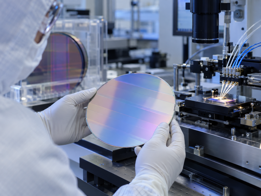
What Is the Difference Between LNOI and TFLN?
The terms LNOI and TFLN are often used interchangeably, but they are not exactly identical.
TFLN, or Thin-Film Lithium Niobate, broadly describes a thin single-crystal lithium niobate device layer used for photonic devices.
LNOI, or Lithium Niobate on Insulator, normally describes a specific wafer structure in which the thin LN layer is bonded to an insulating layer, usually SiO₂, which is then supported by a handle substrate.
A typical structure is:
Thin-film LiNbO₃ / SiO₂ BOX / Handle Wafer
The handle material may be silicon, quartz, lithium niobate or another engineered substrate.
The high refractive-index contrast between lithium niobate and SiO₂ enables strong optical confinement and compact waveguide structures compared with conventional bulk lithium niobate waveguides.
As a result, LNOI has become a particularly attractive platform for photonic integrated circuits.
Why LNOI Wafer Selection Matters More as TFLN Moves Toward Volume Manufacturing
Early thin-film lithium niobate devices were often fabricated on relatively small wafers using research-scale lithography.
That is changing.
In 2026, demonstrations have extended TFLN heterogeneous integration to 200 mm photonics platforms. Research presented at OFC 2026 demonstrated TFLN and SiN heterogeneous integration on a 200 mm silicon-photonics platform, while other work demonstrated TFLN modulators on 200 mm wafers with bandwidth reaching 110 GHz.
At the same time, X-FAB and LIGENTEC have announced plans to scale TFLN-on-SiN and TFLN-on-SOI technologies within a 200 mm foundry environment.
This transition makes substrate specifications increasingly important.
For a research chip, a small variation in LN thickness may sometimes be compensated during device development.
For wafer-scale production, however, variations in:
LN thickness,
BOX thickness,
surface roughness,
wafer flatness,
crystal orientation,
and bonding quality
can translate directly into device variation and lower fabrication yield.
The Basic LNOI Wafer Stack
A conventional LNOI wafer contains three principal layers.
Lithium Niobate Device Layer
This is the functional optical layer where waveguides, resonators and modulators are fabricated.
Buried Oxide Layer
The SiO₂ layer provides optical isolation between the LN device layer and the handle substrate.
It is often referred to as the BOX, or buried oxide.
Handle Substrate
The handle provides mechanical support.
Common choices include:
- ซิลิคอน
- ควอตซ์
- Lithium niobate
Each changes the optical, microwave, thermal and manufacturing behavior of the wafer.
Commercial and research LNOI structures vary significantly. Recent published device platforms, for example, have used LN layers from approximately 300 nm to 700 nm, with buried oxide layers ranging from around 2 μm to approximately 4.7 μm depending on the design.
These numbers should be treated as application examples, not universal LNOI standards.
X-Cut vs Z-Cut LNOI: Which Should You Choose?
Crystal orientation is one of the first parameters that should be defined in an LNOI RFQ.
Lithium niobate is anisotropic.
Its optical and electro-optic properties depend on the relationship between:
- Crystal axis
- Optical propagation direction
- Optical polarization
- Applied electric field
The largest electro-optic coefficient of lithium niobate, r33, is normally highly desirable for electro-optic modulators.
However, how the device accesses r33 depends strongly on wafer orientation.
X-Cut LNOI
X-cut LNOI is widely used for high-speed electro-optic modulators.
In an X-cut configuration, the crystal z-axis lies approximately within the wafer plane.
This allows designers to place electrodes beside the optical waveguide and create a strong in-plane electric field aligned with the lithium niobate z-axis.
The configuration can provide strong overlap between the RF electric field and TE-like optical modes, enabling efficient use of the r33 electro-optic coefficient.
This makes X-cut especially attractive for:
high-speed Mach-Zehnder modulators,
microwave photonics,
coherent optical communications,
photonic computing,
electro-optic frequency combs,
and many RF-photonic circuits.
A large proportion of recent high-performance TFLN modulator research therefore uses X-cut wafers.
Recent examples include commercial X-cut LNOI structures with approximately 500–600 nm LN device layers on Si handles.
Z-Cut LNOI
In Z-cut lithium niobate, the crystal z-axis is normal to the wafer surface.
The electro-optic field configuration is therefore fundamentally different.
Z-cut wafers can be advantageous for structures where vertical electric fields, particular polarization arrangements or nonlinear optical interactions are required.
They have been extensively studied for:
nonlinear optical devices,
microresonators,
frequency conversion,
periodically poled lithium niobate structures,
and selected electro-optic device geometries.
Earlier LNOI research commonly used Z-cut films with TM-type optical configurations to access r33.
Modern device architectures are more diverse, so Z-cut should not simply be considered “inferior” to X-cut.
The correct choice depends on the optical mode, electrode geometry and nonlinear interaction required.
A Practical X-Cut vs Z-Cut Decision
For a customer developing a conventional high-speed traveling-wave electro-optic modulator, X-cut is often the first orientation to evaluate.
For nonlinear optics, periodic poling or devices designed around different electric-field configurations, Z-cut may be preferable.
The correct question is therefore not:
“Is X-cut better than Z-cut?”
It is:
“Which orientation allows the device to use the required electro-optic or nonlinear tensor component with the desired waveguide and electrode geometry?”
How Thick Should the LN Device Layer Be?
LN film thickness directly affects optical confinement, effective refractive index, mode profile, etching depth and waveguide geometry.
There is no universal optimum thickness.
Common research and commercial TFLN devices frequently use submicron LN films.
Published examples include:
approximately 300 nm,
360 nm,
500 nm,
600 nm,
and 700 nm.
Thinner LN Films
A thinner film can support tighter control over mode structure and may be useful for hybrid integration.
However, very thin films may increase fabrication sensitivity.
Small deviations in thickness can cause relatively larger changes in effective refractive index.
Etch-depth control also becomes increasingly important.
Thicker LN Films
A thicker LN device layer can provide stronger optical confinement and greater freedom in ridge-waveguide design.
However, multimode behavior, etching requirements and sidewall control must be considered.
Therefore, device-layer thickness should be selected together with:
wavelength,
waveguide width,
etch depth,
slab thickness,
cladding,
and required optical polarization.
Why LN Thickness Uniformity Matters
When ordering TFLN wafers, nominal thickness alone is not sufficient.
Consider two wafers both specified as:
LN thickness = 600 nm.
If one wafer varies only slightly across the usable area while another contains substantial thickness variation, their photonic performance may be very different.
Thickness variations can change:
- Effective refractive index
- Phase matching
- Resonator wavelength
- Dispersion
- Coupling strength
- Modulator characteristics
- Nonlinear conversion efficiency
This becomes especially important for large wafer diameters and wafer-scale fabrication.
For resonators and wavelength-sensitive photonic devices, thickness uniformity can sometimes be as important as the nominal device-layer thickness.
What Does the BOX Layer Do?
The buried oxide separates the high-index LN layer from the handle wafer.
Its first major function is optical isolation.
If the BOX is too thin, part of the guided optical mode can interact with the handle substrate.
This is particularly important when the handle is silicon because silicon has a much higher refractive index than silica.
A sufficiently thick oxide layer is therefore normally required to suppress substrate leakage.
Recent TFLN-on-silicon device demonstrations have used oxide layers of several micrometers. Examples include 2 μm and 4.7 μm BOX structures.
A recent analysis of TFLN-on-silicon also notes that a several-micrometer oxide layer is typically used to isolate the optical mode from the high-index silicon substrate.
Should You Always Choose a Thicker BOX?
Not necessarily.
Increasing oxide thickness may improve optical isolation from the handle, but the BOX also interacts with:
- RF electrode design
- Microwave effective index
- การระบายความร้อน
- Bonding process
- ความเค้นเชิงกล
- Fabrication integration
For high-speed electro-optic modulators, the entire LN/SiO₂/handle stack can influence microwave propagation.
Therefore, BOX thickness should ideally be selected together with electromagnetic simulation of the traveling-wave electrode.
A specification such as:
“BOX ≥ 2 μm”
may be insufficient for a demanding RF-photonic design.
The buyer should instead define or evaluate the actual device stack.
Silicon Handle LNOI
Silicon is one of the most common handle materials for LNOI.
Its advantages include compatibility with semiconductor processing infrastructure, mechanical robustness and convenient integration with silicon-based photonics platforms.
Numerous recent high-performance TFLN devices use LN/SiO₂/Si structures.
Silicon handles are particularly attractive when the project is intended to interact with:
- Silicon photonics
- SiN photonics
- CMOS-compatible processing
- Wafer-scale lithography
- การรวมแบบไม่เหมือนกัน
However, silicon also influences microwave and optical behavior.
Because silicon has a high refractive index, sufficient BOX thickness is important for suppressing optical leakage.
For traveling-wave modulators, substrate conductivity and dielectric properties must also be considered.
Quartz Handle TFLN
Quartz is increasingly interesting for very-high-frequency electro-optic modulators.
Its low microwave loss can be beneficial when traveling-wave electrodes operate at tens or hundreds of gigahertz.
A recent 4-inch X-cut TFLN-on-quartz platform used a 360 nm LN film and 2.5 μm BOX and demonstrated electro-optic modulator bandwidth above 110 GHz. The researchers highlighted the low microwave absorption of the quartz handle as an important part of the RF design.
Quartz can therefore be attractive for:
ultra-high-speed modulators,
millimeter-wave photonics,
microwave photonics,
and applications where RF substrate loss is critical.
However, quartz should not automatically be considered better than silicon.
The substrate changes both optical and microwave mode behavior, and processes optimized for TFLN-on-silicon cannot always be transferred directly to TFLN-on-quartz.
LN Handle Substrate
Another option is an LN handle wafer.
Using lithium niobate for both the device and handle layers offers good thermal-expansion compatibility.
This can be useful from a bonding and thermomechanical perspective.
However, optical isolation still depends on the intermediate oxide structure, and the wafer may not provide the same CMOS-integration benefits as a silicon handle or the same RF advantages as quartz.
The handle material should therefore be selected according to the complete device architecture rather than a single material property.
Silicon or Quartz Handle: Which Is Better?
A simplified decision framework is:
Choose silicon when the priority is semiconductor process compatibility, heterogeneous integration and established photonics fabrication infrastructure.
Consider quartz when very-low microwave loss and extremely high modulation bandwidth are central device requirements.
But for serious device development, the substrate should be included directly in RF and optical simulation.
The handle is not merely a mechanical support.
It is part of the electromagnetic structure.
Surface Roughness: A Critical LNOI Specification
Low-loss nanophotonic waveguides require high-quality LN surfaces and etched sidewalls.
Surface irregularities can contribute to optical scattering.
The incoming wafer therefore needs a high-quality polished device surface before waveguide fabrication begins.
For photonic-grade LNOI, buyers should request information such as:
surface roughness,
measurement area,
AFM scan size,
surface defect condition,
and polishing method.
A roughness value without specifying measurement conditions is difficult to compare.
For example, an RMS value measured over a very small AFM scan cannot automatically be compared with a result obtained over a much larger area.
Surface Quality Is More Than Ra or RMS
An LNOI wafer can have an excellent average roughness value while still containing isolated defects.
Important surface conditions may include:
- รอยขีดข่วน
- Pits
- Particles
- Haze
- Polishing marks
- ชิป Edge
- Local bonding defects
This is particularly important because waveguide devices may occupy a large fraction of the wafer.
Random localized defects can reduce usable die yield even if average surface roughness is excellent.
Bonding Quality and Interface Defects
Many LNOI wafers are produced through ion slicing and wafer bonding.
In simplified form, a thin single-crystal LN layer is separated from a donor wafer and transferred onto an oxidized handle substrate.
The transferred interface must therefore be evaluated carefully.
Potential issues can include:
bonding voids,
interface particles,
local delamination,
film stress,
and thickness nonuniformity.
For high-value photonics wafers, it can be useful to request a wafer-level bonding inspection rather than relying only on visible surface inspection.
Why Wafer Flatness Also Matters for LNOI
As LNOI moves toward stepper lithography and larger wafer formats, conventional semiconductor geometry parameters become more important.
Relevant parameters can include:
- ทีวี
- โบว์
- วาร์ป
- Edge exclusion
- Device-layer thickness uniformity
Excessive substrate deformation can affect lithography focus, wafer chucking and alignment.
This becomes particularly important for 150 mm and 200 mm processing.
The photonics industry is now actively demonstrating lithium-niobate processing on 200 mm platforms, making wafer-scale geometry increasingly relevant to production rather than only substrate research.
Choosing LNOI for High-Speed Electro-Optic Modulators
For a high-speed Mach-Zehnder modulator, a typical starting point might include:
X-cut LN,
submicron LN device layer,
SiO₂ BOX,
and either a silicon or quartz handle.
But the final stack should be optimized according to:
optical wavelength,
electrode spacing,
waveguide geometry,
target VπL,
microwave impedance,
microwave index,
RF loss,
and required bandwidth.
For very-high-frequency designs, handle material can become especially important.
Choosing LNOI for Nonlinear Photonics
For second-harmonic generation, frequency conversion, optical parametric processes and periodically poled structures, additional considerations become important.
These include:
crystal orientation,
domain engineering,
quasi-phase matching,
LN thickness,
dispersion,
waveguide dimensions,
and propagation direction.
In such applications, X-cut versus Z-cut should be selected based on the nonlinear tensor and desired phase-matching scheme rather than modulator conventions.
Choosing LNOI for Quantum Photonics
Quantum photonic circuits may combine:
- Nonlinear photon generation
- Phase modulation
- High-Q resonators
- Low-loss routing
- Periodic poling
LNOI is attractive because electro-optic control and nonlinear optical generation can potentially be integrated on the same platform.
Integrated lithium-niobate devices are also part of the broader development of scalable quantum photonic hardware.
For these systems, low propagation loss and device uniformity can be more important than simply minimizing wafer cost.
Choosing LNOI for Heterogeneous Photonics
An increasingly important direction is combining TFLN with other photonics platforms.
Examples include:
TFLN + SiN
TFLN + silicon photonics
TFLN + passive low-loss waveguides
TFLN + lasers or detectors
Wafer-scale TFLN integration with SiN has already been demonstrated, including bonding of TFLN material onto larger SiN photonic wafers.
In 2026, 200 mm heterogeneous TFLN integration has further strengthened this direction.
For heterogeneous integration, buyers should pay special attention to:
LN film thickness,
bonding interface,
wafer diameter,
wafer flatness,
alignment requirements,
thermal budget,
and compatibility with downstream semiconductor processes.
Recommended LNOI Wafer RFQ Parameters
An RFQ should avoid simply stating:
“Need LNOI wafer for photonics.”
A more useful inquiry should specify the following parameters.
วัสดุ
LiNbO₃ on insulator / TFLN
เส้นผ่านศูนย์กลางของเวเฟอร์
For example: 3 inch, 4 inch, 6 inch or other required size
ทิศทางของผลึก
X-cut / Z-cut / Y-cut if required
LN film thickness
Nominal value and allowable tolerance
LN thickness uniformity
Specify if critical
BOX material
Usually SiO₂
BOX thickness
Nominal value and tolerance
Handle substrate
Si / Quartz / LN / other
Handle thickness
Nominal value and tolerance
สภาพพื้นผิว
CMP / optical polish / device-grade
ความหยาบของพื้นผิว
Specify measurement method and scan area
Wafer geometry
TTV / Bow / Warp as required
Edge specification
Edge profile and exclusion area
Crystal composition
Congruent LN or other required composition
การใช้สารกระตุ้น
Undoped or MgO-doped if required
Bonding inspection
Specify whether wafer-level void inspection is required
การสมัคร
Electro-optic modulator / nonlinear photonics / quantum photonics / resonator / microwave photonics / other
Providing the application is especially useful because the supplier can help identify whether the requested wafer stack is suitable.
Incoming Inspection of LNOI Wafers
For development and production wafers, incoming inspection can include verification of:
wafer diameter and thickness,
crystal orientation,
LN film thickness,
LN film uniformity,
BOX thickness,
surface roughness,
surface defects,
bow and warp,
bonding voids,
and edge condition.
For demanding photonic projects, buyers may also request wafer maps showing film-thickness distribution.
This information becomes increasingly useful when comparing device performance across different regions of a wafer.
Do Not Specify LNOI Based Only on the Lowest Roughness
One common procurement mistake is comparing LNOI wafers using only one attractive specification.
ตัวอย่างเช่น:
Supplier A: lower surface roughness.
Supplier B: slightly higher roughness.
It may appear that Supplier A automatically offers the better wafer.
But Supplier B may provide:
better LN thickness uniformity,
fewer bonding defects,
lower wafer bow,
more stable crystal orientation,
or better lot-to-lot repeatability.
For integrated photonics, yield depends on the complete wafer stack.
A single specification cannot represent overall substrate quality.
What Information Should You Give the Supplier?
For a custom or research LNOI project, providing the intended device application can significantly improve wafer selection.
Useful information includes:
Operating wavelength
Optical polarization
Waveguide type
Target LN thickness
Target etch depth
Modulator or passive device
Electrode configuration
RF bandwidth
Required wafer diameter
Preferred handle material
Whether periodic poling is required
Whether wafer-scale lithography will be used
Whether the wafer will undergo bonding or heterogeneous integration
This allows the substrate specification to be matched to the actual photonic design.
สรุป
Selecting an LNOI or TFLN wafer for integrated photonics requires much more than choosing a lithium niobate film thickness.
X-cut versus Z-cut determines how the device interacts with lithium niobate’s anisotropic electro-optic and nonlinear properties.
LN film thickness controls optical confinement, mode structure and waveguide design.
BOX thickness influences optical isolation and can also affect RF behavior.
Handle substrate affects mechanical support, optical leakage, microwave propagation, thermal behavior and process compatibility.
Surface roughness and bonding quality influence propagation loss and fabrication yield.
And as thin-film lithium niobate moves toward larger wafer formats and 200 mm heterogeneous photonics manufacturing, film uniformity, flatness and wafer-level consistency are becoming increasingly important.
The best LNOI wafer is therefore not simply the wafer with the thinnest film, thickest BOX or lowest quoted surface roughness.
It is the wafer stack whose crystal orientation, optical structure, substrate and dimensional tolerances are matched to the final photonic device and fabrication process.
For electro-optic modulators, nonlinear photonics, quantum photonics or heterogeneous photonic integration, defining these parameters clearly at the RFQ stage can significantly reduce process-development risk and improve device yield.