
With the rapid development of advanced electronics and optoelectronic devices, wide-bandgap materials such as sapphire (Al₂O₃) and silicon carbide (SiC) have become essential substrates. However, their exceptional hardness and brittleness present significant challenges during wafer singulation. Traditional mechanical dicing methods often induce defects that reduce device yield. Laser dicing technology has emerged as a high-precision, low-damage alternative, significantly improving yield and process reliability. This article provides a scientific overview of how laser dicing enhances yield in sapphire and SiC wafer processing, focusing on mechanisms, advantages, and industrial implications.
1. Inledning
Sapphire and SiC wafers are widely used in applications such as LEDs, power electronics, RF devices, and optical systems. Both materials exhibit:
- High hardness (Mohs hardness: sapphire ~9, SiC ~9.5)
- High brittleness
- Low fracture toughness
These properties make them extremely difficult to dice using conventional blade-based methods, where chipping, cracking, and contamination are common. Yield loss during dicing can exceed 5–15% depending on wafer thickness and device density.
Laser dicing technology addresses these limitations by enabling non-contact material removal, significantly reducing mechanical stress and improving die integrity.
2. Limitations of Traditional Dicing Methods
2.1 Mechanical Blade Dicing
Blade dicing relies on diamond-coated blades rotating at high speeds. While effective for silicon, it introduces several issues for sapphire and SiC:
- Kantflisning: Micro-fractures propagate along crystalline planes
- Kerf loss: Wide cutting lanes reduce usable wafer area
- Tool wear: Frequent blade replacement increases cost
- Contamination: Coolants and debris affect surface cleanliness
2.2 Impact on Yield
Defects introduced during dicing can lead to:
- Reduced die strength
- Electrical failure due to microcracks
- Lower packaging reliability
As device dimensions shrink and wafer value increases (especially for 6-inch and 8-inch SiC wafers), minimizing dicing-induced damage becomes critical.
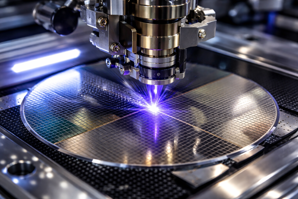
3. Principles of Laser Dicing Technology
Laser dicing uses focused laser beams to modify or remove material along predefined scribe lines. The main approaches include:
3.1 Ablation-Based Laser Dicing
- Material is directly vaporized by high ენერგy pulses
- Suitable for thin wafers
- May introduce a small heat-affected zone (HAZ)
3.2 Stealth Dicing (SD)
- Laser is focused inside the wafer to create a modified layer
- External force (e.g., expansion tape) separates the dies
- No surface damage or debris
3.3 Laser Grooving + Mechanical Breaking
- Laser creates precise grooves
- Minimal mechanical force required for separation
4. Mechanisms of Yield Improvement
4.1 Reduction of Mechanical Stress
Laser dicing is a non-contact process, eliminating mechanical loading on the wafer. This prevents:
- Crack initiation
- Skador under markytan
- Wafer warping
Result: Higher die survival rate.
4.2 Narrower Kerf Width
Typical comparison:
| Metod | Kerf Width (µm) | Impact |
|---|---|---|
| Blade dicing | 30–50 | Higher material loss |
| Dicing med laser | 10–20 | More dies per wafer |
A narrower kerf directly increases the number of usable dies, improving overall yield per wafer.
4.3 Minimal Edge Chipping
Laser processing enables smooth and clean edges, particularly important for brittle materials like sapphire and SiC. Reduced chipping leads to:
- Improved mechanical strength
- Better reliability during packaging and operation
4.4 Lower Thermal Damage
Advanced laser systems (e.g., picosecond and femtosecond lasers) minimize heat diffusion:
- Ultra-short pulse duration reduces HAZ
- Prevents phase transformation or oxidation
- Maintains material properties
This is especially critical for SiC devices used in high-power environments.
4.5 Debris-Free Processing
Stealth dicing and optimized laser parameters can achieve near zero debris generation, reducing:
- Surface contamination
- Cleaning requirements
- Risk of particle-induced defects
5. Process Optimization for Sapphire and SiC
5.1 Sapphire Wafer Dicing
Key considerations:
- High transparency requires wavelength optimization
- UV or green lasers are commonly used
- Stealth dicing is particularly effective for LED substrates
Outcome:
- Crack-free edges
- High optical quality retention
5.2 SiC Wafer Dicing
Utmaningar:
- Hög värmeledningsförmåga
- Strong covalent bonding
Solutions:
- Use of ultrafast lasers (picosecond/femtosecond)
- Multi-pass scanning strategies
Outcome:
- Minskade mikrosprickor
- Improved die strength for power devices
6. Yield Improvement: Quantitative Perspective
Typical improvements observed in industrial settings:
| Parameter | Bladet Dicing | Dicing med laser |
|---|---|---|
| Edge chipping rate | 5–10% | <1% |
| Die strength | Måttlig | Hög |
| Yield loss (dicing stage) | 5–15% | <3% |
| Kerf loss | Hög | Låg |
These improvements translate directly into higher profitability, especially for high-value SiC wafers used in electric vehicles and renewable energy systems.
7. Industrial Implications
Laser dicing technology is becoming a standard solution in advanced wafer processing due to:
- Compatibility with thin wafers (<100 µm)
- Suitability for high-density device layouts
- Integration with automated production lines
As wafer sizes increase (6-inch → 8-inch SiC, and beyond), the economic benefits of improved yield become even more significant.
8. Challenges and Future Trends
Despite its advantages, laser dicing still faces challenges:
- High initial equipment cost
- Process parameter complexity
- Throughput limitations for thick wafers
Future developments include:
- AI-driven process optimization
- Hybrid dicing technologies
- Higher-power ultrafast laser systems
9. Conclusion
Laser dicing technology represents a transformative advancement in the processing of sapphire and SiC wafers. By eliminating mechanical stress, reducing kerf loss, minimizing defects, and improving edge quality, it significantly enhances wafer yield and device reliability. As demand for high-performance electronics continues to grow, laser dicing will play a crucial role in enabling cost-effective and scalable manufacturing of next-generation semiconductor devices.