
Semiconductor manufacturing lies at the heart of modern electronics, powering everything from smartphones to data centers. The process of turning a raw silicon wafer into a fully functional integrated circuit is extraordinarily complex, involving hundreds of precise steps that require specialized equipment. Each piece of equipment not only impacts chip performance and yield but also determines the efficiency, reliability, and cost of the manufacturing line. Understanding the workflow and the role of each type of wafer processing equipment is critical for engineers, manufacturers, and industry professionals.
1. Wafer Preparation and Cleaning Equipment
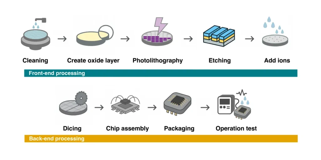
The first stage of wafer processing is preparing and cleaning the silicon wafers:
- Wafer inspection systems verify the surface quality and detect defects in raw wafers.
- Cleaning equipment removes particles, organic residues, and native oxides using chemical solutions, megasonic baths, or high-purity water.
- Drying systems ensure that wafers are free of moisture, which is critical for subsequent photolithography and thin-film deposition.
Maintaining ultra-clean wafer surfaces is essential because even microscopic contamination can cause defects in later stages, reducing chip yield and reliability.
2. Thin-Film Deposition Equipment
After cleaning, wafers undergo thin-film deposition, a process that builds the multiple layers needed for semiconductor devices:
- Chemical Vapor Deposition (CVD) produces insulating or semiconducting layers, such as silicon dioxide (SiO₂) and silicon nitride (Si₃N₄). CVD ensures uniform coverage across the wafer surface and within high-aspect-ratio structures.
- Physical Vapor Deposition (PVD), including sputtering, deposits metal layers used for interconnects and contacts.
- Atomic Layer Deposition (ALD) enables precise, atomically controlled films, which are essential for advanced nodes below 10nm.
Each deposition technique requires highly controlled temperatures, vacuum conditions, and gas flow parameters to ensure film uniformity and reproducibility.
3. Photolithography Equipment
Photolithography defines the circuit patterns on the wafer. It is one of the most critical steps in wafer fabrication, as it directly determines feature size and device density:
- Spin coaters apply a uniform layer of photoresist on the wafer surface.
- Mask aligners and stepper systems project ultraviolet (UV) or extreme ultraviolet (EUV) light through photomasks to expose the resist.
- Developers selectively remove exposed or unexposed areas of photoresist, revealing the desired circuit patterns.
Advanced lithography tools, including EUV scanners, achieve nanometer-scale resolution and high overlay accuracy, enabling the production of modern high-performance processors.
4. Etching Equipment
After lithography, etching equipment transfers the photoresist patterns into the underlying layers:
- Dry etching systems, such as Reactive Ion Etching (RIE) and Inductively Coupled Plasma (ICP) etching, use plasma to remove material anisotropically.
- Wet etching equipment employs chemical solutions to dissolve specific materials isotropically.
Etching requires precise control over gas composition, plasma power, and temperature to achieve consistent feature depth, critical dimension (CD), and profile across the wafer.
5. Chemical Mechanical Planarization (CMP) Equipment
As multiple layers are deposited and patterned, wafers become topographically uneven. CMP equipment restores a flat surface:
- Mechanical polishing pads combined with chemical slurries remove high points and planarize the wafer surface.
- Flatness and surface smoothness are crucial for subsequent lithography steps to maintain focus and alignment.
CMP is particularly important for advanced nodes and multi-layer interconnects where surface irregularities can degrade device performance.
6. Doping and Thermal Processing Equipment
Doping introduces controlled amounts of impurities to modify semiconductor properties:
- Diffusion furnaces allow dopants to penetrate the silicon lattice at high temperatures.
- Rapid Thermal Processing (RTP) systems perform short-duration heating for dopant activation, oxidation, and annealing.
Thermal processing equipment requires tight temperature uniformity and precise timing to ensure consistent electrical characteristics across all devices on the wafer.
7. Inspection and Metrology Equipment
High-yield manufacturing relies on inspection and metrology systems:
- Optical and electron microscopes detect surface defects and measure critical dimensions.
- Film thickness monitors ensure deposited layers meet design specifications.
- Overlay and alignment tools verify that successive layers align accurately.
These systems provide real-time feedback to optimize processes and minimize defects, enabling continuous improvement and high wafer yield.
8. Wafer Handling and Automation Systems
Modern fabs operate with high levels of automation to reduce contamination risk and improve throughput:
- Automated Material Handling Systems (AMHS) transport wafers between process tools without manual contact.
- Robotic wafer handlers and FOUPs ensure precise, contamination-free movement.
- Integrated process control software monitors and schedules equipment operations to maximize efficiency.
Automation not only improves productivity but also enhances repeatability and reduces variability caused by human handling.
9. Final Testing and Packaging
Once wafer processing is complete, wafers are tested and prepared for chip packaging:
- Probe stations test the electrical characteristics of each die.
- Wafer dicing saws separate individual chips.
- Packaging equipment encapsulates chips in protective materials and connects them to external interfaces.
Quality inspection continues throughout packaging to ensure that only fully functional chips reach customers.
Conclusão
The transformation from a silicon wafer to a finished chip involves a complex chain of specialized equipment, each performing a critical role in deposition, patterning, etching, planarization, doping, inspection, and automation. Precision, stability, and cleanliness at every step are essential to achieve high yields and reliable semiconductor devices.
As the industry advances toward smaller nodes, 3D structures, and new materials like SiC and GaN, the requirements for wafer processing equipment will continue to increase. Understanding the workflow and the role of each piece of equipment is essential for manufacturers, engineers, and supply chain professionals aiming to stay at the forefront of semiconductor technology.