
Consumables inside a plasma etch chamber are continuously exposed to reactive radicals, energetic ions, heat, RF fields and repeated cleaning cycles. Focus rings, electrodes, showerheads, liners, windows, insulators and wafer-support components may gradually erode, change surface condition or release particles during operation.
Material selection therefore affects more than component lifetime. It can also influence plasma uniformity, process drift, wafer contamination, chamber-cleaning frequency and production yield.
Silicon, chemical vapor deposited silicon carbide, quartz and alumina are all widely used in semiconductor process equipment. However, they are not interchangeable. The correct material depends on the plasma chemistry, component location, electrical function, acceptable contamination elements and total operating cost.
This guide compares silicon, CVD SiC, quartz and alumina and explains how semiconductor equipment manufacturers and fabs can select suitable consumables for plasma etch chambers.
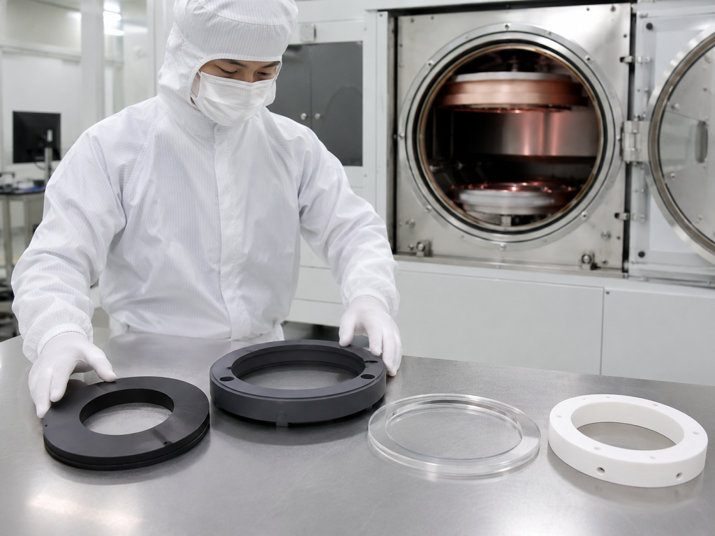
Why Plasma-Facing Material Selection Matters
During dry etching, the wafer is not the only surface exposed to plasma. Chamber walls and internal components can also undergo physical ion bombardment and chemical reactions.
As these components erode, they may produce:
- Microscopic particles
- Nonvolatile fluoride deposits
- Surface roughening
- Metallic or elemental contamination
- Changes in chamber impedance
- Plasma-distribution changes
- Process drift between maintenance cycles
Research on semiconductor plasma chambers shows that component erosion and particle generation are closely connected to material chemistry, surface condition and plasma exposure. High-density fluorine-containing plasma is especially demanding because it can react with chamber materials while ion bombardment removes or fractures the resulting surface layer.
A suitable chamber material should therefore provide a balance of:
- Plasma resistance
- Low particle generation
- Low contamination risk
- Suitable electrical properties
- Thermal stability
- 치수 정밀도
- Practical manufacturing cost
No single material provides the best result in every chamber position.
Quick Comparison of the Four Materials
| 재료 | 주요 장점 | Main Limitations | 일반적인 애플리케이션 |
|---|---|---|---|
| 실리콘 | Compatible with silicon processing, controllable conductivity, low risk of foreign metallic contamination | Can erode relatively quickly in aggressive plasma, brittle and consumable | Focus rings, edge rings, electrodes, cover rings |
| CVD SiC | High purity, good thermal performance, dense structure, long potential service life | Higher cost, difficult machining, longer lead time | Electrodes, focus rings, showerheads, liners, high-duty plasma-facing parts |
| 쿼츠 | High purity, dielectric, transparent and suitable for optical or RF-related functions | Limited erosion resistance in some fluorocarbon plasmas, possible Si–O–F particle formation | Windows, rings, liners, shields, insulating parts |
| 알루미나 | Strong electrical insulation, mechanical strength, mature ceramic manufacturing and cost efficiency | May form aluminum-fluoride-related surface products and particles in fluorine plasma | Insulators, supports, chamber structures, rings, liners and shielded components |
This table is only a starting point. Final selection must consider the actual gas chemistry and where the component is located relative to the plasma.
1. Silicon Consumables
High-purity monocrystalline or polycrystalline silicon is commonly used for focus rings, edge rings, electrodes and other components surrounding a silicon wafer.
Advantages of Silicon
Process-material compatibility
For silicon wafer etching, silicon consumables introduce an element already present in the wafer and process environment. This can be preferable to introducing aluminum or other foreign elements into a contamination-sensitive process.
In fluorine-containing plasma, silicon can react to form volatile silicon fluoride species. This behavior can help reduce the accumulation of certain solid reaction products compared with materials that form less volatile fluorides. Silicon and SiC are consequently used as plasma-facing materials where contamination control is important.
Adjustable electrical properties
Silicon can be supplied with controlled resistivity and doping type. This is useful when the component participates in RF coupling, bias distribution or electrical grounding.
A buyer may need to specify:
- N-type or P-type
- Resistivity range
- Single-crystal or polycrystalline structure
- 결정 방향
- Bulk purity
- Surface resistivity uniformity
정밀 가공
Silicon rings and plates can be machined to tight dimensional tolerances using established semiconductor processing methods. Notches, grooves, holes, steps and complex edge profiles can be incorporated into the design.
Limitations of Silicon
Silicon is intentionally treated as a consumable in many plasma systems. Direct exposure can gradually change its dimensions and surface profile.
발생할 수 있는 문제로는 다음과 같은 것들이 있습니다:
- Inner-diameter enlargement
- Focus-ring height reduction
- Edge-profile changes
- Surface roughening
- Localized erosion
- Reduced plasma uniformity near the wafer edge
- Shorter replacement intervals
Silicon is also brittle. Thin sections, deep holes and sharp internal corners may crack during machining, installation or thermal cycling.
When to Select Silicon
Silicon is often suitable when:
- The process wafer is silicon-based
- Low foreign-element contamination is required
- The component is expected to be replaced periodically
- Electrical conductivity must be controlled
- High dimensional precision is required
- Initial component cost is more important than maximum lifetime
It is frequently used for focus rings, cover rings and electrodes in etch chambers processing silicon wafers.
2. CVD Silicon Carbide Consumables
CVD SiC is produced by depositing silicon carbide from gaseous precursors onto a substrate or mandrel. The resulting material can have high purity, high density and a fine, controlled microstructure.
Advantages of CVD SiC
High purity and low porosity
High-quality CVD SiC can be produced with very low impurity content and without the sintering additives used in some conventional ceramic materials.
A dense, low-porosity structure helps reduce:
- Particle trapping
- Gas absorption
- Localized plasma attack
- Cleaning residue
- Weak grain-boundary erosion
Thermal performance
SiC provides good thermal conductivity compared with quartz and alumina. This can help control temperature gradients in electrodes, rings and other parts exposed to plasma heating.
Stable temperature is important because component temperature can affect:
- Surface reaction rates
- Polymer deposition
- Plasma chemistry
- Dimensional stability
- Etch repeatability
Potentially longer service life
SiC is commonly selected for demanding plasma-facing components because of its mechanical strength, wear resistance and durability.
However, buyers should not assume that every SiC grade has identical erosion resistance. Research comparing different SiC microstructures shows that erosion behavior can vary significantly with manufacturing method, grain size and crystallographic characteristics. One study reported that a large-grain PVT SiC focus-ring material had higher erosion resistance than the tested CVD SiC material under its specific process conditions.
The correct conclusion is therefore not that CVD SiC is universally the most resistant material, but that properly specified SiC can provide strong performance when its grade and microstructure match the plasma environment.
Limitations of CVD SiC
CVD SiC components are normally more expensive than silicon, quartz or standard alumina parts.
Cost is influenced by:
- Deposition time
- Material thickness
- Component diameter
- Machining complexity
- 표면 마감
- 구멍 개수
- 평탄도 요구 사항
- Inspection level
CVD SiC is also hard and difficult to machine. Deep slots, small holes and thin walls can increase lead time and manufacturing risk.
Repair or dimensional reworking after use may also be limited.
When to Select CVD SiC
CVD SiC should be considered when:
- The component is directly exposed to high-density plasma
- Long maintenance intervals are valuable
- High purity is required
- Thermal conductivity is important
- The part has a critical effect on plasma distribution
- Particle reduction justifies a higher initial cost
- Repeated component replacement causes excessive downtime
Typical components include electrodes, showerheads, focus rings, edge rings and plasma-facing liners.
3. Quartz Consumables
Quartz glass is widely used in semiconductor processing because of its purity, dielectric behavior, optical transmission and thermal stability.
Common quartz chamber components include:
- Dielectric windows
- Viewports
- Cover rings
- Shadow rings
- Liners
- Shields
- Insulating spacers
- Gas-distribution components
Advantages of Quartz
전기 절연
Quartz is an electrical insulator and can be useful where conductive materials would disturb the RF field or create an unwanted electrical path.
광학적 투명도
Quartz may be selected when the chamber requires:
- Optical endpoint detection
- Plasma observation
- Laser access
- Optical emission monitoring
- Visual inspection
High chemical purity
Semiconductor-grade fused quartz can be manufactured with low metallic impurity levels. This makes it useful for clean processing environments when the plasma chemistry is compatible.
Thermal stability
Quartz has low thermal expansion and good thermal-shock behavior compared with many conventional glasses. It is used throughout semiconductor thermal and plasma equipment in tubes, rings, windows and process fixtures.
Limitations of Quartz
Quartz should not automatically be selected for every direct plasma-facing position.
Studies of quartz in fluorocarbon plasma have reported surface roughening and the formation of silicon-oxide and fluoride-containing reaction products. These products may develop into particles as exposure continues.
Its limitations become more important under:
- High-density ICP plasma
- High RF power
- Strong ion bombardment
- Fluorocarbon chemistry
- Long process exposure
- Strict particle specifications
Quartz may perform well as a window, shield or component positioned away from the most aggressive ion path, while showing an unacceptable replacement rate as a directly exposed focus ring.
When to Select Quartz
Quartz is usually appropriate when:
- Electrical insulation is required
- Optical transmission is necessary
- The component is not in the highest-erosion zone
- High purity is important
- The process chemistry has proven compatibility
- A lower-cost precision glass component is preferred
- Complex fused or welded structures are needed
The plasma-facing area and expected erosion rate should still be evaluated before production use.
4. Alumina Ceramic Consumables
Alumina is one of the most established engineering ceramics used in semiconductor equipment. High-purity alumina components can provide electrical insulation, mechanical strength and dimensional stability at a practical cost.
Advantages of Alumina
Strong electrical insulation
Alumina is frequently used for:
- Electrical isolators
- RF insulators
- Supports
- Spacers
- Feedthrough structures
- Structural ceramic parts
It can maintain mechanical integrity while electrically separating conductive chamber components.
Mature manufacturing process
Alumina can be formed through pressing, isostatic pressing, casting and machining. It is generally more economical than CVD SiC for large or structurally complex parts.
Mechanical strength
Dense alumina provides good hardness and wear resistance. It is suitable for components that must withstand assembly loads, repeated maintenance and mechanical contact.
Limitations of Alumina
In fluorine-containing plasma, alumina can react to form aluminum-fluoride-containing surface layers. Physical ion bombardment may then remove portions of the reacted layer and contribute to particle generation.
Research has linked fluorine-plasma exposure of alumina-based chamber surfaces with Al–F reaction products and contamination particles.
The erosion performance of alumina also depends on:
- 순도
- 밀도
- 다공성
- Grain size
- Secondary phases
- 표면 마감
- Coating quality
Dense, high-purity material generally performs more uniformly than porous or impurity-rich alumina because pores and weak microstructural regions can become localized erosion sites.
For highly aggressive plasma environments, alumina parts may be protected with yttria, yttrium oxyfluoride or another plasma-resistant coating. Coating adhesion, porosity, thickness uniformity and refurbishment strategy then become important specifications.
When to Select Alumina
Alumina is suitable when:
- Electrical insulation is the primary requirement
- The component is partly shielded from direct plasma
- Structural strength is important
- Cost must be controlled
- The chamber design already uses qualified alumina grades
- A plasma-resistant coating can be applied where required
Typical uses include supports, insulators, chamber liners, spacers, rings and structural ceramic components.
Material Selection by Chamber Component
Focus rings and edge rings
The focus ring directly affects the plasma and electric-field distribution around the wafer edge. Dimensional erosion can influence edge-die uniformity.
Common choices include:
- Silicon: Good process compatibility and controlled conductivity
- CVD SiC: Considered when longer life and thermal stability justify higher cost
- Quartz: Suitable only for qualified chemistries and lower-exposure designs
- Alumina: More commonly used when insulation is required and contamination risk is acceptable
For critical focus-ring applications, silicon and SiC are usually evaluated first.
Electrodes and showerheads
Electrodes and showerheads may require:
- Electrical conductivity
- High-purity material
- Uniform gas holes
- Tight flatness
- Thermal control
- Stable surface condition
Silicon and CVD SiC are frequently selected for plasma-facing conductive components.
CVD SiC may provide longer potential service life, while silicon can offer lower initial cost and compatibility with silicon processes.
Dielectric windows
Quartz and alumina are more likely to be considered for dielectric windows.
Quartz is advantageous when optical transmission is required. Alumina may be preferred when optical access is unnecessary and greater mechanical strength or a specific dielectric design is required.
The designer should evaluate:
- RF transmission
- 두께
- Temperature gradient
- Plasma exposure
- Coating compatibility
- Window cooling
- Vacuum sealing
Chamber liners and shields
Liners may be made from quartz, alumina, silicon or SiC depending on the process.
The choice should reflect whether the liner is intended to:
- Protect the chamber wall
- Collect process deposition
- Control contamination
- Stabilize chamber seasoning
- Provide electrical isolation
- Reduce maintenance time
A removable quartz liner may be economical for one process, while a SiC liner may be justified for another process with severe erosion and costly downtime.
Insulators and structural supports
Alumina is often the most practical choice for electrical insulators and structural ceramic supports.
Quartz may also be used when purity, thermal expansion or optical properties are more important than mechanical strength.
How Plasma Chemistry Changes Material Selection
Fluorine-containing plasma
Fluorine-based chemistries can react strongly with silicon-containing and aluminum-containing materials, but the volatility and stability of the reaction products differ.
The selection must consider:
- Reaction-product volatility
- Surface-layer stability
- Polymer deposition
- Ion energy
- Chamber temperature
- Particle sensitivity
Silicon and SiC may be attractive where volatile silicon fluoride formation reduces certain contamination risks. Quartz and alumina require careful evaluation because fluorinated surface products can contribute to roughness or particle generation under aggressive conditions.
Chlorine-containing plasma
Chlorine-based plasma may produce different corrosion and contamination mechanisms. A material that performs poorly in fluorine plasma may behave differently in chlorine plasma.
Selection should be based on actual chamber testing rather than a general material ranking.
Oxygen plasma
Oxygen plasma can remove carbon-containing films but may also change SiC surface chemistry or interact with deposited chamber films.
The effect depends on RF power, temperature, process pressure and whether oxygen is used alone or in a mixed gas.
Mixed fluorocarbon plasma
Fluorocarbon plasma may create polymer layers on chamber components. Polymer thickness can either temporarily protect the surface or create unstable deposits that later flake and generate particles.
Surface finish and chamber-cleaning conditions are therefore as important as bulk material composition.
Seven Questions to Ask Before Selecting a Material
1. Which elements are prohibited?
Determine the contamination budget for:
- Aluminum
- Sodium
- Potassium
- Iron
- Calcium
- Boron
- Carbon
- Oxygen
- Other trace metals
A material with long lifetime may still be unsuitable if its erosion products introduce prohibited elements.
2. Is the component conductive or insulating?
Do not select material based only on corrosion resistance. The component may need to:
- Conduct RF current
- Maintain electrical isolation
- Control bias
- Prevent arcing
- Support capacitive coupling
Silicon and SiC can be engineered for conductive functions, while quartz and alumina are primarily insulating materials.
3. Where is the component located?
A component positioned in the direct ion path experiences different conditions from a shielded support behind a liner.
Define:
- Distance from wafer
- Plasma density
- Ion-bombardment direction
- Local temperature
- Gas-flow exposure
- Deposition tendency
4. How does dimensional erosion affect the process?
For a focus ring, a small height change may affect edge uniformity. For a simple shield, greater erosion may be acceptable.
Critical dimensions should be linked to replacement criteria.
5. What cleaning process will be used?
Consumables may be exposed to:
- In-situ plasma cleaning
- Wet chemical cleaning
- 초음파 세척
- High-pressure water
- Thermal baking
- Mechanical bead blasting
A material must survive both the production plasma and the maintenance process.
6. What is the real lifecycle cost?
The lowest-priced part may not provide the lowest operating cost.
Lifecycle analysis should include:
- 구매 가격
- 설치 시간
- Chamber downtime
- Cleaning frequency
- Process recalibration
- Wafer scrap risk
- Replacement interval
- Refurbishment possibility
7. Can the supplier control surface condition?
Two components with the same material name may perform differently because of:
- 표면 거칠기
- 표면 아래 손상
- 다공성
- Grain structure
- Cleaning residue
- 엣지 치핑
- Machining contamination
Material grade and finishing process should therefore be specified together.
Recommended RFQ Information
When requesting a quotation for plasma etch chamber consumables, provide:
- Component name and drawing
- Equipment model or chamber position
- Current component material
- Requested material or materials for comparison
- Plasma chemistry
- Typical RF power range
- Operating pressure and temperature
- Direct or indirect plasma exposure
- Required electrical resistivity
- Material purity requirement
- Prohibited contamination elements
- Surface roughness requirement
- 평탄도 및 평행도
- Hole diameter and position tolerance
- Edge-chipping limit
- Cleaning method
- Inspection-report requirements
- Required quantity
- 예상 수명
- Current failure or erosion problem
Used-component photographs and erosion measurements are especially helpful when replacing an existing chamber consumable.
Final Selection Guide
Choose silicon when process compatibility, controlled conductivity, precise machining and manageable replacement cost are the main priorities.
Choose CVD SiC when high purity, thermal performance and longer maintenance intervals justify a higher component cost, while confirming that the selected SiC grade is qualified for the actual plasma chemistry.
Choose quartz when electrical insulation, optical transmission, high purity or complex fused structures are required, provided that direct fluorocarbon-plasma erosion is acceptable.
Choose alumina when electrical insulation, structural strength and cost efficiency are important, especially for supports or shielded components. For direct fluorine-plasma exposure, consider a qualified high-purity grade or protective coating.
In many etch chambers, the best design uses several materials rather than one material throughout the chamber. A silicon focus ring, CVD SiC electrode, quartz window and alumina insulator may each perform a different function in the same system.
결론
Silicon, CVD SiC, quartz and alumina each offer valuable properties for plasma etch chamber consumables, but material selection must be based on the exact operating environment.
The most important factors are:
- Plasma chemistry
- Component position
- Contamination limits
- Electrical function
- Thermal conditions
- Dimensional erosion
- Cleaning method
- Lifecycle cost
A successful selection process compares not only the bulk material, but also purity, microstructure, surface finish, machining quality and inspection requirements.
Before replacing an existing component with another material, manufacturers should review the complete chamber function and, where possible, perform controlled qualification testing. This reduces the risk of solving a lifetime problem while unintentionally creating a contamination, plasma-uniformity or particle-generation problem.
자주 묻는 질문
Is CVD SiC always better than silicon for focus rings?
아니요. CVD SiC may provide higher durability and thermal stability, but silicon can offer better cost efficiency, process compatibility and easier dimensional replacement. SiC performance also varies with material grade and microstructure.
Why is silicon commonly used in plasma etch chambers?
Silicon is compatible with silicon wafer processing, can be supplied with controlled electrical resistivity and can form volatile reaction products in fluorine-containing plasma. It is also available in high-purity semiconductor grades.
Can quartz be used as a plasma-facing material?
Yes, but its suitability depends on the plasma chemistry and exposure level. Quartz can erode and generate reaction products in aggressive fluorocarbon plasma, so it is often better suited to windows, shields and lower-exposure positions.
Is alumina suitable for fluorine plasma?
Alumina can be used, but direct fluorine-plasma exposure may form aluminum-fluoride-containing surface layers and particles. High-purity dense alumina or plasma-resistant coatings may be needed for demanding applications.
Which material has the lowest particle risk?
There is no universal answer. Particle performance depends on plasma chemistry, surface finish, material density, component geometry and cleaning history. The material must be qualified under the actual chamber conditions.
Can a quartz or alumina component be replaced directly with SiC?
Not always. Changing material may alter electrical behavior, thermal distribution, RF coupling and plasma uniformity. The chamber design and component function should be reviewed before substitution.