
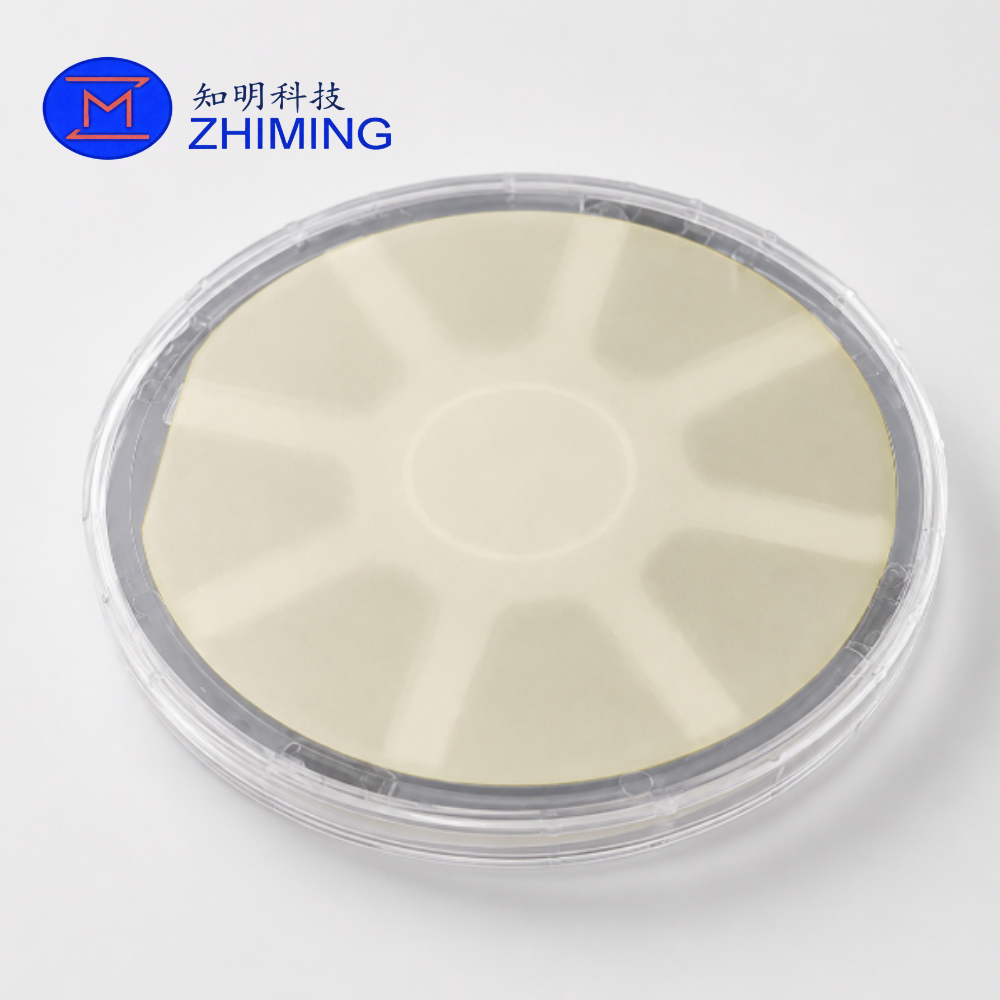
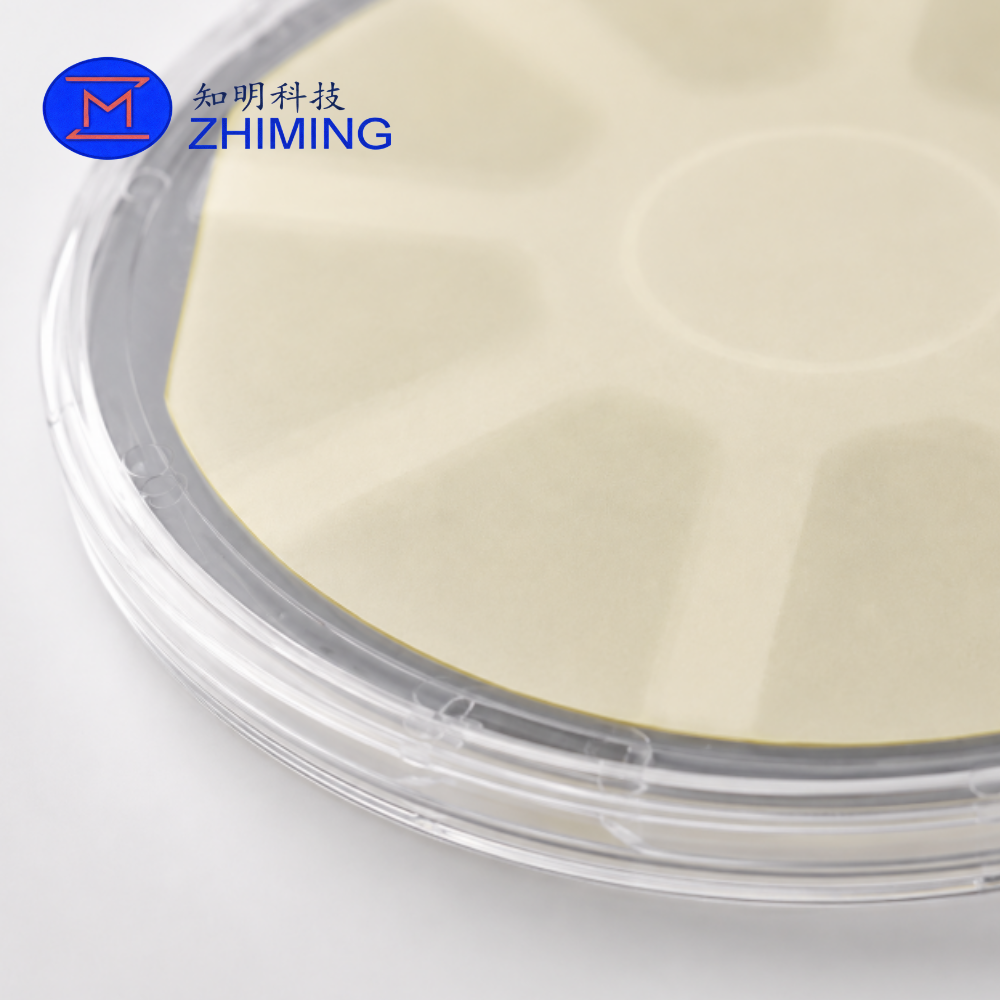
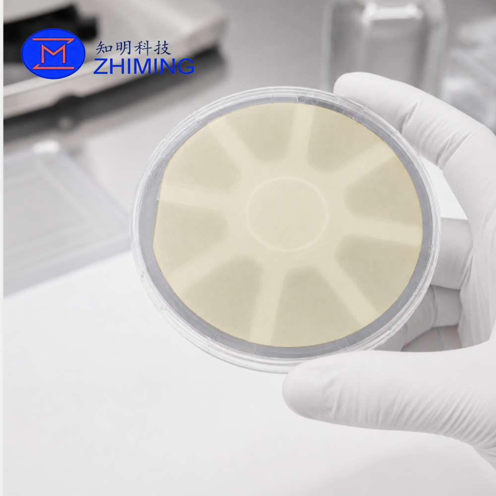
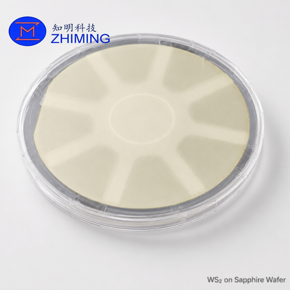
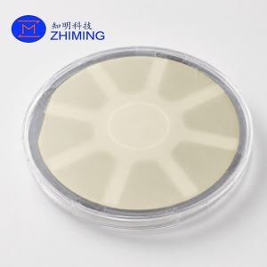
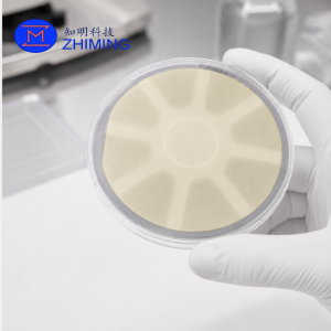
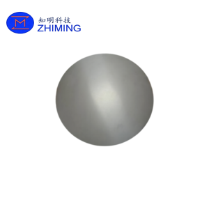
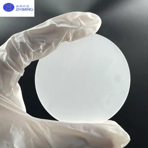
 WS₂ on Sapphire Wafer is a high-quality two-dimensional semiconductor material consisting of a continuous tungsten disulfide (WS₂) thin film grown on a sapphire substrate. As a member of the Transition Metal Dichalcogenide (TMD) family, WS₂ has emerged as one of the most promising materials for next-generation electronics, optoelectronics, photodetectors, sensors, and nano-scale devices.
Combining the excellent electronic and optical properties of WS₂ with the superior thermal stability and transparency of sapphire, this product provides a reliable platform for advanced material research, device fabrication, and semiconductor development.
ZMSH supplies research-grade WS₂ on sapphire wafers with excellent crystal quality, smooth surface morphology, high uniformity, and comprehensive characterization data.
 主な特徴
主な特徴
- Continuous multilayer WS₂ film
- High crystal quality with hexagonal structure
- Excellent wafer-scale uniformity
- RMS surface roughness around 0.11 nm
- Strong photoluminescence response
- Sapphire substrate with superior thermal stability
- Available in 2-inch and 4-inch wafers
- Suitable for semiconductor and optoelectronic applications
- Custom specifications available
仕様
| 項目 | 仕様 |
|---|---|
| Product Name | WS₂ on Sapphire Wafer |
| 素材 | Tungsten Disulfide |
| Chemical Formula | WS₂ |
| Material Category | 2D Semiconductor Material |
| 基板材料 | サファイア(Al₂O₃) |
| ウエハーサイズ | 2 Inch, 4 Inch |
| Film Type | Multilayer Continuous Film |
| 結晶構造 | Hexagonal |
| 表面粗さ | RMS ≈ 0.11 nm |
| 均一性 | High Wafer-Scale Uniformity |
| Characterization | AFM, Raman, PL, PL Mapping, TEM, GIXRD, GI-WAXS |
| Customization | 利用可能 |
 Why Choose WS₂ on Sapphire?
As conventional semiconductor technologies approach scaling limitations, two-dimensional materials have become an important direction for future device research. WS₂ offers a suitable bandgap, strong light-matter interaction, and excellent carrier transport characteristics, making it highly attractive for advanced electronic and photonic devices.
The sapphire substrate provides:
- High mechanical strength
- Excellent thermal resistance
- Chemical stability
- Optical transparency
- Low surface defect density
Compared with exfoliated flakes, wafer-scale WS₂ films provide greater consistency, better reproducibility, and improved compatibility with semiconductor processing.
Product Advantages
Excellent Crystal Quality
The WS₂ film exhibits a highly ordered crystal structure verified through advanced characterization techniques, ensuring reliable performance for research and device fabrication.
Smooth Surface Morphology
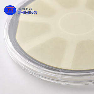
AFM measurements demonstrate an ultra-flat surface with RMS roughness around 0.11 nm, supporting nanoscale device processing and characterization.
Strong Optical Properties
High photoluminescence intensity and narrow spectral linewidth indicate superior optical quality and uniform film growth.
Wafer-Scale Uniformity
Uniform film coverage enables repeatable experiments and large-area device fabrication, reducing sample-to-sample variation.
Reliable Sapphire Platform
The sapphire substrate offers excellent stability during high-temperature processing and optical testing.
代表的なアプリケーション
2D Semiconductor Research
Used for studying electronic transport, band structure engineering, carrier dynamics, and low-dimensional semiconductor physics.
Photodetectors
Suitable for visible and near-infrared photodetection research due to the strong optical absorption and photoresponse of WS₂.
光電子デバイス
Applicable to light-emitting devices, optical sensors, modulators, and integrated photonic systems.
Advanced Transistor Research
Provides a platform for developing ultra-thin channel devices and next-generation field-effect transistors.
Gas Sensors
The high surface sensitivity of WS₂ makes it an attractive material for gas detection and environmental monitoring.
Biosensors
Suitable for biochemical sensing applications requiring high sensitivity and rapid response.
Flexible Electronics Research
Can serve as a material growth and transfer platform for future flexible and wearable electronic devices.
Academic and Industrial R&D
Widely used by universities, national laboratories, semiconductor institutes, and emerging technology companies.
Available Products
| Product Type | ウエハーサイズ |
| Standard WS₂ on Sapphire | 2 Inch |
| Standard WS₂ on Sapphire | 4 Inch |
| Research Grade WS₂ Wafer | Custom |
| Customized WS₂ Wafer | Custom |
Customization Services
To meet different research and development requirements, ZMSH offers customized solutions including:
- Custom wafer diameters
- Different substrate materials
- Film thickness adjustment
- Research-grade specifications
- Special crystal orientation requirements
- Customized characterization reports
Please contact our technical team for detailed specifications and project support.
Quality Characterization
Every batch can be supplied with material characterization data including:
- Optical Microscopy
- Atomic Force Microscopy (AFM)
- Raman Spectroscopy
- Photoluminescence (PL)
- PL Mapping
- Transmission Electron Microscopy (TEM)
- Grazing Incidence X-Ray Diffraction (GIXRD)
- Grazing Incidence Wide-Angle X-Ray Scattering (GI-WAXS)
These characterization methods help verify film quality, crystal structure, surface morphology, and optical performance.
よくあるご質問
What is WS₂?
WS₂ (Tungsten Disulfide) is a layered transition metal dichalcogenide semiconductor widely used in two-dimensional material research and advanced electronic devices.
Why is sapphire used as the substrate?
Sapphire provides excellent thermal stability, optical transparency, chemical resistance, and mechanical strength, making it an ideal substrate for high-quality WS₂ growth.
What wafer sizes are available?
Standard products are available in 2-inch and 4-inch wafers. Customized sizes can be discussed based on project requirements.
Can characterization reports be provided?
Yes. Material characterization reports such as AFM, Raman, PL, GIXRD, and GI-WAXS can be supplied upon request.
Do you support customized specifications?
Yes. We offer customized wafer sizes, substrate options, film structures, and other specifications according to customer requirements.

レビュー
レビューはまだありません。