
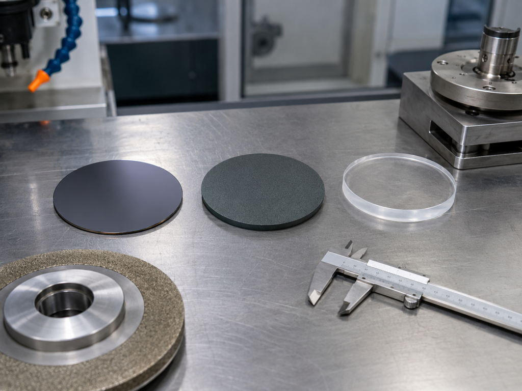
When single-crystal silicon, silicon carbide, and sapphire are placed on the same machining table, the first question many people ask is simple: which one is the hardest?
For a machining engineer, however, hardness is only one part of the story.
The real question is more complex: which material is the most difficult to process while maintaining efficiency, yield, tool life, dimensional accuracy, and surface quality at the same time?
The answer is not always obvious. Single-crystal silicon, sapphire, and silicon carbide are all hard and brittle materials used in high-value industries. They are found in semiconductor wafers, optical windows, LED substrates, power devices, sensors, precision instruments, and advanced electronic components. Each material has its own machining challenges.
Single-crystal silicon is difficult because the crystal must remain structurally perfect. Sapphire is difficult because many applications require an almost flawless optical surface. Silicon carbide is difficult because it combines high hardness, brittleness, strong tool wear, low material removal efficiency, and strict mass-production requirements.
From the perspective of overall production machining difficulty, silicon carbide is usually the most challenging of the three.
It is not difficult because of one single property. It is difficult because almost every contradiction in hard and brittle material machining appears together in SiC.
Machining Difficulty Is Not Only About Hardness
Hardness is often the first property people compare. In general, harder materials are more resistant to scratching, indentation, and wear. But in precision manufacturing, a hard material is not automatically the most difficult material to machine.
Machining difficulty depends on several factors:
- How fast material can be removed
- How quickly tools or grinding wheels wear out
- How easily cracks or edge chipping form
- How deep subsurface damage extends
- How difficult it is to polish the surface
- How strict the final flatness, roughness, and dimensional tolerances are
- How stable the process is in mass production
For example, a material may not be extremely hard, but if it is highly sensitive to internal crystal damage, the process becomes difficult. Another material may be very hard but can be processed into a simple shape with looser tolerances. A third material may require high throughput, low defect density, long tool life, and nanometer-level surface quality at the same time. That is where the real challenge begins.
This is why single-crystal silicon, sapphire, and silicon carbide should not be judged only by hardness. They should be compared by their complete machining behavior.
Single-Crystal Silicon: The Challenge Is Protecting the Crystal
Single-crystal silicon is the foundation of integrated circuits, MEMS devices, solar cells, and many semiconductor components. Compared with sapphire and silicon carbide, silicon is not the hardest material. In many machining operations, it is easier to remove than SiC or sapphire.
But silicon has a different problem: it is highly sensitive to internal damage.
During slicing, grinding, thinning, lapping, polishing, and edge processing, silicon wafers must maintain excellent flatness and surface integrity. The visible surface is only one part of the requirement. Beneath the surface, micro-cracks, residual stress, dislocations, amorphous layers, and lattice damage can all affect later device performance.
These defects may not be obvious immediately after machining. A wafer can look smooth and clean, yet still contain subsurface damage. In semiconductor manufacturing, these hidden defects may become serious problems during lithography, thin-film deposition, ion implantation, thermal processing, bonding, packaging, or device operation.
For silicon wafers, the challenge is not simply to remove material. The challenge is to remove material while keeping the crystal as undamaged as possible.
This is why silicon processing usually involves controlled cutting, precision grinding, chemical mechanical polishing, cleaning, inspection, and strict process control. The goal is not only a smooth surface, but also low damage depth, low stress, stable thickness, and reliable wafer geometry.
In short, single-crystal silicon is difficult because it demands crystal-level integrity.
Sapphire: The Challenge Is Leaving No Machining Trace
Sapphire is single-crystal aluminum oxide. It is widely used in LED substrates, optical windows, watch crystals, infrared windows, laser components, sensors, protective covers, and high-end consumer electronics.
The biggest advantage of sapphire is its excellent hardness, wear resistance, chemical stability, and optical transparency. These properties make it ideal for applications where glass or plastic would scratch, haze, deform, or degrade too quickly.
But the same hardness that makes sapphire durable also makes it difficult to machine.
Sapphire grinding and polishing require diamond tools, careful process control, and long processing time. Cutting too aggressively may cause edge chipping, cracks, pits, or subsurface damage. Polishing too slowly increases cost and reduces productivity. If the part is used as an optical window or lens cover, even a tiny scratch, pit, or polishing mark may affect appearance, light transmission, scattering, or imaging performance.
This is especially important for optical-grade sapphire components. A sapphire window for a sensor, camera, laser system, or infrared device cannot simply be “dimensionally correct.” It must also have a highly controlled surface finish, good parallelism, proper flatness, low defect density, and clean edges.
The challenge of sapphire is therefore not only material removal. It is surface perfection.
A sapphire component may be mechanically acceptable but optically unacceptable. That is why sapphire processing often includes multiple stages: rough shaping, fine grinding, edge finishing, lapping, polishing, cleaning, coating, and inspection. Each step must avoid introducing damage that later becomes difficult or expensive to remove.
In short, sapphire is difficult because it requires a mirror-grade, low-damage, visually clean surface.
Silicon Carbide: The Challenge Is That Every Requirement Is Strict
Silicon carbide is a key material for power electronics, electric vehicles, fast charging, photovoltaic inverters, high-temperature devices, RF devices, and advanced semiconductor systems. It offers excellent thermal conductivity, high breakdown electric field, high-temperature stability, chemical stability, and mechanical strength.
These properties make SiC extremely valuable. They also make it extremely difficult to process.
From a machining perspective, silicon carbide is almost a complete set of hard and brittle material problems.
First, SiC is very hard. This causes rapid wear of diamond tools, grinding wheels, saw wires, and polishing consumables. Tool wear is not only a cost issue. It also affects process stability, surface roughness, cutting force, heat generation, and dimensional accuracy.
Second, SiC is brittle. If cutting or grinding forces fluctuate, edge chipping, micro-cracks, brittle pits, and subsurface damage can occur. The surface may appear acceptable after grinding, but the damage layer underneath may still require further removal.
Third, SiC is chemically stable. This is excellent for device performance and harsh-environment use, but it makes polishing more difficult. Removing damage from SiC can require longer polishing times and more advanced process chemistry.
Fourth, SiC wafers are expensive. A low-yield process is not acceptable. Every wafer represents significant material value, so machining defects directly increase cost.
Fifth, demand is growing. With the expansion of electric vehicles, power modules, and high-efficiency energy systems, SiC processing must not only be high quality. It must also be scalable, stable, and efficient.
This creates the core contradiction of SiC machining:
If the process is too aggressive, damage increases.
If the process is too conservative, efficiency drops.
If the tool wears too quickly, process consistency becomes unstable.
If polishing time is too long, cost rises.
If damage is not fully removed, device yield may suffer.
This is why silicon carbide is often considered the most difficult material among the three from a mass-production viewpoint.
Why SiC Is Harder to Balance Than Silicon and Sapphire
Single-crystal silicon, sapphire, and SiC all require precision processing, but their difficulties are different.
Silicon is mainly about protecting the crystal structure and controlling wafer damage. Sapphire is mainly about achieving an optical-grade surface without visible defects. SiC requires both damage control and surface quality, while also dealing with severe tool wear and mass-production efficiency.
That makes SiC more difficult to balance.
For silicon, decades of semiconductor manufacturing have created mature process routes. The industry has strong experience in wafer slicing, grinding, polishing, cleaning, and inspection.
For sapphire, the processing chain is also well understood, especially for optical windows, LED substrates, and watch crystals. The cost may be high, but many sapphire applications accept a slower polishing process because the final value is in durability and optical performance.
For SiC, the situation is more demanding. Power semiconductor manufacturing needs larger wafers, lower defect levels, better flatness, lower surface damage, and higher output. At the same time, SiC remains difficult to grind and polish efficiently.
This is why SiC machining is not simply a “hard material” problem. It is a manufacturing economics problem. The final process must achieve quality, yield, throughput, and cost control at the same time.
Key Machining Problems in Silicon Carbide
The first major problem is tool wear. Diamond tools are commonly used for SiC machining, but even diamond tooling can wear rapidly under high load. As the tool wears, the cutting edge changes. This may increase grinding force, heat, vibration, and surface roughness.
The second problem is edge chipping. SiC wafers and components can chip during cutting, grinding, drilling, or edge profiling. Edge defects may later become crack initiation points, especially during handling, bonding, thermal cycling, or device processing.
The third problem is subsurface damage. In brittle-mode material removal, cracks can extend below the visible surface. Even if the surface looks flat, hidden damage may remain. Removing this layer requires additional grinding, lapping, polishing, or chemical mechanical polishing.
The fourth problem is heat. Grinding and cutting generate frictional heat. Local heat can increase stress and accelerate tool wear. In hard and brittle materials, heat and mechanical stress often interact, increasing the risk of damage.
The fifth problem is process window control. Feed rate, wheel speed, abrasive size, grinding depth, coolant condition, tool dressing, vibration, and fixture design all influence the final result. A small change in parameter settings may affect surface roughness, crack formation, and tool life.
This is why SiC machining requires more than a powerful machine. It requires a controlled system.
Why Ultrasonic-Assisted Machining Is Becoming Important
For materials like silicon carbide, simply increasing machine power or wheel speed is not always the best answer. More force can remove material faster, but it can also increase cracks, heat, edge chipping, and tool wear.
Ultrasonic-assisted machining offers another approach.
In this process, high-frequency micro-vibration is introduced into cutting, grinding, drilling, or milling. Instead of continuous contact between the tool and workpiece, the tool engages the material in a rapid intermittent manner. This can reduce the average cutting force, improve coolant access, help chip removal, reduce frictional heat, and make the removal process more controllable.
For hard and brittle materials, this is valuable because damage is often caused by excessive localized stress. If stress concentration can be reduced, the risk of brittle fracture and subsurface cracking may also be reduced.
Ultrasonic assistance is not magic. It does not make SiC easy to process. Parameters such as vibration amplitude, frequency, spindle speed, feed rate, tool type, abrasive size, depth of cut, and coolant strategy still need careful optimization.
In some cases, a moderate ultrasonic amplitude may improve surface quality, while excessive amplitude may introduce impact marks or new defects. Therefore, ultrasonic-assisted machining should be understood as a process optimization tool, not a universal shortcut.
Its real value is helping manufacturers find a better balance between efficiency and material integrity.
How to Choose the Right Processing Strategy
For single-crystal silicon, the machining strategy should focus on low damage depth, stable wafer geometry, and clean surface preparation for semiconductor processes. Damage inspection, stress control, and polishing consistency are critical.
For sapphire, the strategy should focus on optical surface quality, scratch control, edge finishing, and coating compatibility. The process must be designed around the final optical function of the component.
For silicon carbide, the strategy must focus on the entire production chain. Cutting, grinding, lapping, polishing, cleaning, and inspection must work together. Tool wear, material removal rate, wafer flatness, subsurface damage, and final yield must all be considered.
A good SiC process is not defined by how fast it removes material in one step. It is defined by whether it can repeatedly produce qualified wafers or components at acceptable cost.
Final Comparison
If we compare only hardness, sapphire and silicon carbide are both far more difficult than single-crystal silicon.
If we compare optical surface requirements, sapphire is extremely demanding.
If we compare crystal damage sensitivity, single-crystal silicon requires very strict control.
But if we compare total production difficulty — including hardness, brittleness, tool wear, surface damage, polishing difficulty, process stability, throughput, and cost — silicon carbide is usually the most difficult material to machine.
Silicon is difficult because the inside of the crystal cannot be damaged.
Sapphire is difficult because the surface cannot show defects.
Silicon carbide is difficult because every part of the process must be controlled at once.
It must be ground, polished, and finished efficiently. It must avoid chipping and cracks. It must protect the surface and subsurface. It must control tool wear. It must support stable mass production.
That is why silicon carbide is not only a difficult material. It is a test of the entire manufacturing system.
Következtetés
Single-crystal silicon, sapphire, and silicon carbide are all important materials in modern technology. Each one is difficult to process in a different way.
Single-crystal silicon tests the ability to protect crystal integrity. Sapphire tests the ability to create a flawless optical surface. Silicon carbide tests the ability to balance hardness, brittleness, tool wear, surface damage, efficiency, and yield.
For research samples or small custom parts, all three materials can be processed successfully with the right equipment and experience. But in mass production, the hardest question is not whether the material can be machined. The real question is whether every piece can be machined consistently, economically, and without hidden damage.
From that perspective, silicon carbide remains the most challenging of the three.
Its machining difficulty is not just a material property. It is a complete manufacturing challenge.