Novinky z oboru Silicon Wafer Coring Guide: Diameter Reduction, Edge Profile, TTV, Bow and Post-Coring Inspection Přečtěte si více »
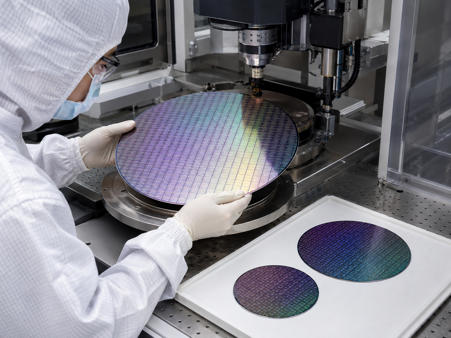
Novinky z oboru Wafer Coring vs Wafer Dicing: How to Choose for 300mm-to-200mm and Custom Diameter Conversion Přečtěte si více »
Novinky ze společnosti Wafer Surface Particle Inspection Guide: Particle Size, Count Limits and Cleanliness Requirements Přečtěte si více »
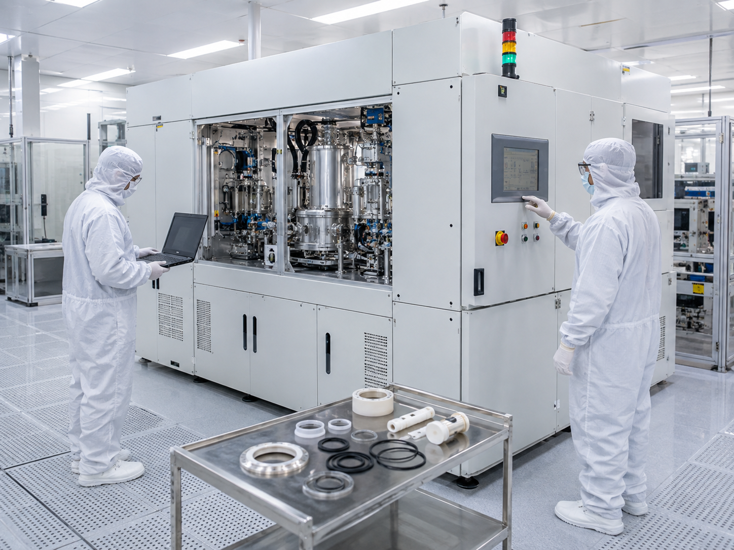
Novinky z oboru Single-Wafer Processing Tools for Advanced Packaging: What Equipment Buyers Should Evaluate Přečtěte si více »
Novinky z oboru How to Qualify Semiconductor Process Equipment: FAT, SAT, Process Window, Uptime and Spare Parts Přečtěte si více »
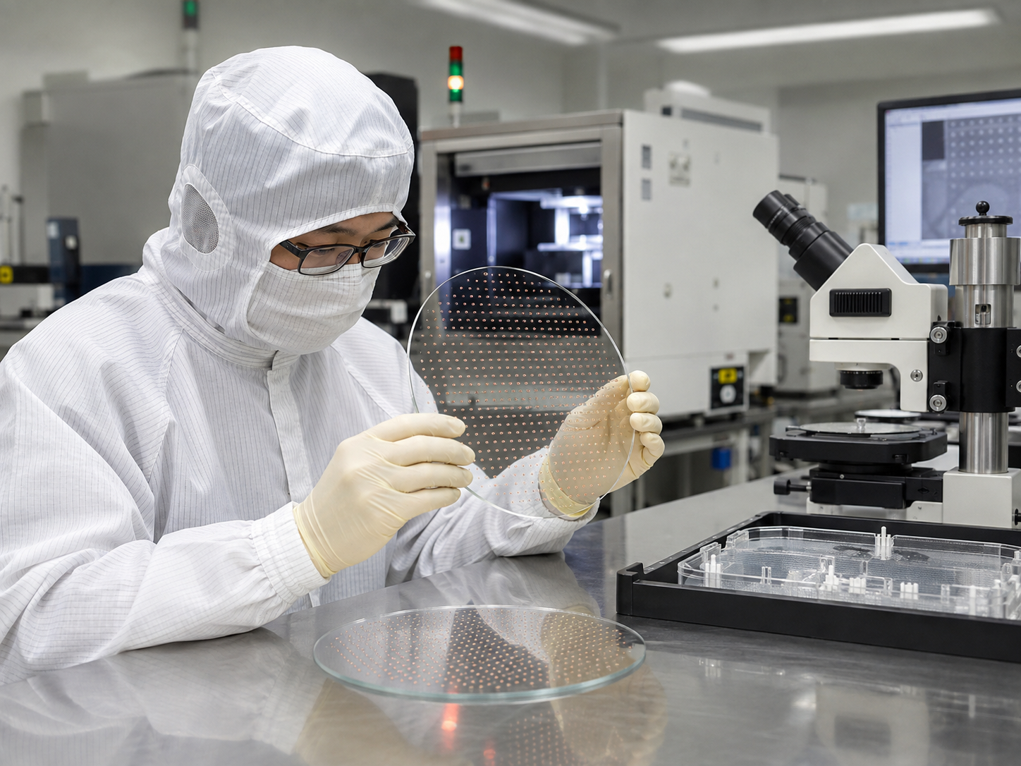
Novinky z oboru TGV Glass Substrate Procurement Checklist: Via Diameter, Pitch, Copper Filling, Warpage and Inspection Přečtěte si více »
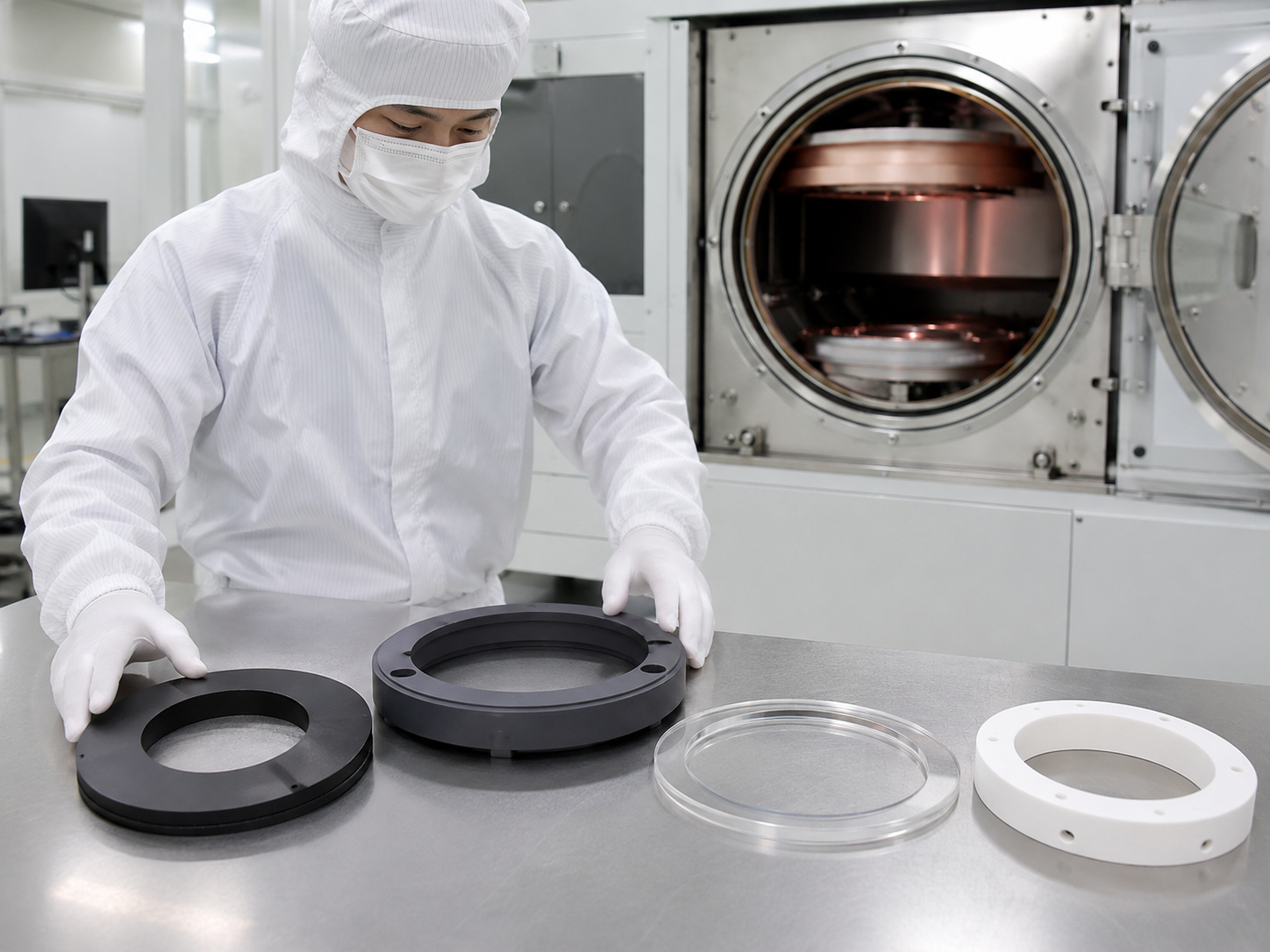
Novinky z oboru Silicon, CVD SiC, Quartz or Alumina: How to Select Consumables for Plasma Etch Chambers Přečtěte si více »
Novinky z oboru Wafer Resizing Service Guide: Converting 300mm Wafers to 200mm, 150mm and Custom Diameters Přečtěte si více »
Technologie a aplikace Wafer Dicing Defect Control: Chipping, Kerf Loss and Edge Quality Přečtěte si více »