
300mm wafer dicing requires more careful planning than small-size wafer cutting because the wafer has a larger surface area, higher material value and stricter handling requirements. Whether the wafer is silicon, glass, sapphire, SiC, quartz or another advanced substrate, a clear RFQ can reduce quotation errors, process risk and quality disputes.
For semiconductor buyers, the goal is not only to ask “Can you cut 300mm wafers?” but to confirm material compatibility, dicing method, kerf width, edge quality, inspection criteria, cleaning and packaging requirements.
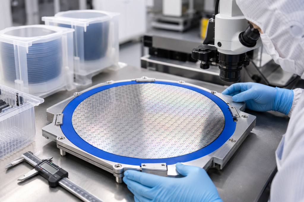
Why 300mm Wafer Dicing Needs a Detailed RFQ
A 300mm wafer is more sensitive to handling, warpage, mounting stability and cutting uniformity. Small process issues can lead to edge chipping, die breakage, particle contamination or lower final yield.
A detailed RFQ helps the supplier understand:
- Wafer material and thickness
- Cutting method requirements
- Final chip or piece size
- Street width and kerf limit
- Edge chip acceptance criteria
- Cleaning and packaging level
- Inspection method
- Quantity and delivery schedule
Without this information, the quotation may be inaccurate or the supplier may select a process that does not match the final application.
1. Wafer Material
The first item to confirm is the wafer material. Different materials require different dicing tools, cutting parameters and handling methods.
Common 300mm wafer materials include:
- Křemík
- Sklo
- Křemík tavený
- Quartz
- Sapphire
- Karbid křemíku
- Ceramic substrates
- Compound semiconductor materials
Silicon is widely processed, but brittle or hard materials such as glass, sapphire and SiC may require slower cutting speed, special blades or laser processing.
2. Wafer Thickness
Thickness directly affects cutting method, blade selection, feed rate and breakage risk. Thin wafers need better support during mounting and cutting, while thick wafers may require multiple passes or special tooling.
Buyers should provide:
- Nominal thickness
- Thickness tolerance
- Whether the wafer is thinned or polished
- Whether the wafer has bow or warp
- Whether temporary bonding or special support is needed
For very thin 300mm wafers, handling and mounting may be as important as the cutting process itself.
3. Final Size and Cutting Layout
The RFQ should clearly define the final part size and cutting layout. If the wafer will be diced into chips, the buyer should provide die size and street width. If it will be cut into custom pieces, a drawing or layout file is required.
Important details include:
- Final die size
- Number of cuts
- Cut direction
- Street width
- Edge exclusion area
- Custom shape requirement
- Orientation mark or notch position
For custom dicing, CAD files or clear drawings help avoid misunderstanding.
4. Dicing Method
Different dicing methods have different advantages. The supplier may choose the method based on material, thickness and edge quality requirement.
Common options include:
- Diamond blade dicing
- Laserové krájení na kostky
- Skryté krájení na kostky
- Scribing and breaking
- Precision cutting for custom substrates
Blade dicing is cost-effective and widely used. Laser dicing can reduce mechanical stress, but thermal effects should be evaluated. For brittle glass or sapphire substrates, the best method should be selected after reviewing the drawing and quality requirement.
5. Kerf Width
Kerf width refers to the material removed during cutting. It affects die size, layout design and material utilization. If the street width is too narrow, dicing defects may increase.
Buyers should confirm:
- Maximum acceptable kerf width
- Street width
- Blade thickness if specified
- Final size tolerance after dicing
- Whether kerf loss affects functional areas
This is especially important for expensive substrates or high-density layouts.
6. Edge Quality and Chipping Limit
Edge quality is one of the most important RFQ items. The buyer should not only ask for “good edge quality” but define measurable requirements.
Recommended items include:
- Maximum top-side chip size
- Maximum back-side chip size
- Sidewall quality requirement
- Micro-crack acceptance
- Corner damage limit
- Whether microscope inspection is required
- Whether sample photos are required before shipment
For semiconductor packaging, MEMS, optical and high-reliability applications, edge quality should be clearly defined before production.
7. Surface Protection and Mounting
During 300mm wafer dicing, mounting stability affects cutting accuracy and defect control. Buyers should confirm whether the wafer surface needs protection.
Possible requirements include:
- Dicing tape type
- UV tape or standard tape
- Protective coating
- Front-side or back-side dicing
- Sensitive surface protection
- Temporary bonding support
If the wafer has devices, coatings or patterned structures, the sensitive side must be clearly marked.
8. Cleanliness and Particle Control
After dicing, particles and residues may remain on the wafer surface or cut edges. For semiconductor applications, cleaning requirements should be defined in the RFQ.
Buyers should confirm:
- Cleaning method
- Particle control requirement
- DI water rinse requirement
- Drying method
- Cleanroom packaging
- Whether post-dicing contamination is critical
For test wafers or dummy wafers, cleanliness requirements may be different from device wafers.
9. Inspection Requirements
Inspection standards should be matched to the application. A simple prototype may only need basic dimensional checks, while semiconductor production parts may require more detailed inspection.
Common inspection items include:
- Final size
- Šířka řezu
- Čipy Edge
- Trhliny
- Škrábance na povrchu
- Particles
- Množství
- Visual photos
- Inspection report
If the buyer needs 100% inspection, this should be stated clearly because it affects cost and delivery time.
10. Packaging and Shipment
300mm wafers and diced parts must be packed carefully to avoid breakage or contamination during shipment.
Packaging options may include:
- Wafer cassette
- Single wafer container
- Gel box
- Vacuum-sealed bag
- Cleanroom bag
- Foam-protected box
- Custom tray
The correct packaging depends on wafer condition, final part size and cleanliness requirement.
300mm Wafer Dicing RFQ Checklist
| RFQ Item | Information to Provide |
|---|---|
| Materiál | Silicon, glass, sapphire, SiC, quartz or other material |
| Průměr | 300mm wafer or custom diameter |
| Tloušťka | Nominal thickness and tolerance |
| Final size | Die size, chip size or custom shape |
| Kresba | CAD file, layout file or technical drawing |
| Dicing method | Blade, laser, stealth dicing or supplier recommendation |
| Street width | Available cutting lane width |
| Šířka řezu | Maximum acceptable kerf |
| Kvalita hran | Chipping limit, cracks, sidewall requirement |
| Surface protection | Tape, coating, sensitive side |
| Cleanliness | Cleaning and particle control requirements |
| Kontrola | Sampling or 100% inspection, report requirement |
| Balení | Cassette, tray, gel box or cleanroom packaging |
| Množství | Prototype or batch order quantity |
| Aplikace | Packaging, MEMS, optics, test wafer or device wafer |
Závěr
A clear 300mm wafer dicing RFQ helps buyers reduce process risk, control cost and improve final yield. Before requesting a quotation, buyers should define material, thickness, final size, dicing method, kerf width, edge quality, inspection and packaging requirements.
For semiconductor buyers, the more complete the RFQ information is, the easier it is for the supplier to recommend a practical dicing process and provide an accurate quotation.
ČASTO KLADENÉ DOTAZY
What information is most important for a 300mm wafer dicing RFQ?
Material, thickness, final size, street width, kerf width, edge chip limit, quantity and drawing are the most important details.
Can 300mm glass wafers be diced?
Yes, but glass is brittle and requires proper tooling, support, cutting parameters and edge inspection.
Is laser dicing better than blade dicing for 300mm wafers?
It depends on the material, thickness, layout and edge quality requirement. Blade dicing is common, while laser dicing may be useful for reducing mechanical stress.
What causes chipping during wafer dicing?
Chipping can be caused by material brittleness, blade wear, high feed rate, poor mounting, insufficient cooling or unsuitable process parameters.
Should buyers provide drawings for wafer dicing?
Yes. Drawings or layout files help confirm cut size, orientation, tolerance and inspection requirements.