
As artificial intelligence (AI), high-performance computing (HPC), cloud data centers, and high-speed communication technologies continue to advance, the demand for more powerful semiconductor devices is growing rapidly. Traditional transistor scaling, which has driven semiconductor progress for decades, is approaching physical and economic limits. As a result, advanced packaging has emerged as one of the most important technologies for sustaining performance improvements beyond Moore’s Law.
Rather than serving only as a protective enclosure for semiconductor devices, advanced packaging has become a key enabler of system-level performance. By integrating multiple chips into a single package and providing high-density interconnections, advanced packaging can significantly improve bandwidth, reduce latency, lower power consumption, and increase overall computing efficiency.
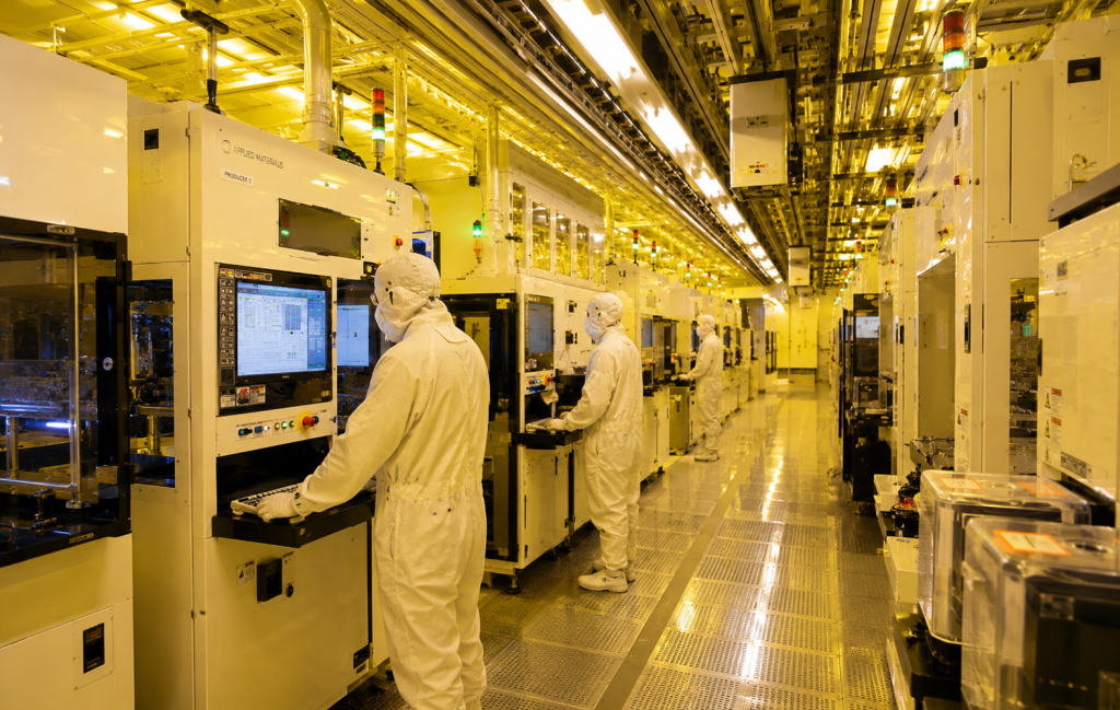
Understanding Advanced Packaging
Conventional packaging technologies typically connect a single chip to a substrate through wire bonding or flip-chip assembly. While these approaches remain suitable for many applications, they are increasingly unable to meet the performance requirements of modern AI processors and high-bandwidth memory systems.
Advanced packaging introduces new integration methods such as Wafer-Level Packaging (WLP), 2.5D packaging, 3D stacking, Through-Silicon Via (TSV) technology, and Chiplet-based heterogeneous integration. These technologies enable multiple semiconductor dies to function as a highly integrated system, delivering significantly higher performance than traditional single-chip solutions.
For AI accelerators and high-performance processors, advanced packaging is no longer an optional enhancement—it has become a fundamental technology for achieving next-generation computing performance.
Hybrid Bonding Equipment: Enabling Ultra-High-Density Interconnections
Hybrid bonding is widely regarded as one of the most important technologies for future 3D integration.
Traditional interconnection methods rely on solder bumps or micro-bumps to connect semiconductor dies. However, as interconnect pitch continues to shrink, these approaches face limitations in electrical performance, thermal management, and scalability.
Hybrid bonding directly joins copper-to-copper and dielectric-to-dielectric surfaces without the need for conventional solder structures. This creates extremely fine-pitch interconnections while reducing parasitic resistance and capacitance.
The process requires exceptional surface flatness, cleanliness, and alignment accuracy. Even microscopic defects can negatively impact bonding quality and yield. Consequently, hybrid bonding equipment represents one of the most technically demanding categories within advanced packaging manufacturing.
CMP Equipment: Achieving Atomic-Level Surface Planarity
Chemical Mechanical Planarization (CMP) is a critical process used to create highly planar surfaces during semiconductor manufacturing.
CMP combines controlled chemical reactions with mechanical polishing to remove material and achieve nanometer-scale flatness. This level of precision is essential for advanced packaging applications, including TSV fabrication, wafer thinning, redistribution layer (RDL) formation, and hybrid bonding.
Without adequate planarization, subsequent processes such as lithography, deposition, and bonding may suffer from reduced accuracy and lower manufacturing yields.
As advanced packaging structures become increasingly complex, CMP continues to play a central role in ensuring process stability and device reliability.
Etching Equipment: Building Three-Dimensional Structures
Etching technology is responsible for creating precise micro- and nano-scale features within semiconductor materials.
In advanced packaging, etching equipment is extensively used for TSV formation, RDL patterning, dielectric layer processing, and various interconnect structures. Among these applications, deep TSV etching is particularly challenging because it requires high aspect ratio structures with excellent dimensional control.
The quality of etched features directly affects electrical performance, thermal behavior, and long-term reliability. As a result, advanced etching systems are indispensable for enabling three-dimensional integration technologies.
Thin-Film Deposition Equipment: Constructing Functional Layers
Advanced packaging relies on the deposition of multiple functional layers throughout the manufacturing process.
These layers may serve as conductors, insulators, diffusion barriers, passivation films, or bonding interfaces. Common deposition techniques include Physical Vapor Deposition (PVD), Chemical Vapor Deposition (CVD), and Atomic Layer Deposition (ALD).
Among them, ALD has gained particular importance because it enables atomic-scale control of film thickness and exceptional uniformity over complex three-dimensional structures.
High-quality thin films are essential for maintaining electrical performance, ensuring mechanical stability, and achieving high manufacturing yields in advanced packaging applications.
Testing Equipment: Ensuring Functional Integrity
As semiconductor packages evolve from single-chip devices to complex multi-die systems, testing requirements have become significantly more demanding.
Modern advanced packaging often integrates processors, memory, and specialized accelerators into a single package. Each component must be thoroughly verified before and after assembly to ensure system functionality.
Testing equipment evaluates electrical characteristics, signal integrity, power consumption, thermal behavior, and long-term reliability. Comprehensive testing helps identify defects early in the manufacturing process and ensures that only fully functional devices reach the final stage of production.
Metrology and Inspection Equipment: The Eyes of the Production Line
Precision measurement and defect inspection are essential throughout advanced packaging manufacturing.
Metrology tools measure critical parameters such as film thickness, feature dimensions, surface topology, alignment accuracy, and mechanical stress. Inspection systems detect particles, voids, cracks, contamination, and other defects that may compromise performance.
As interconnect dimensions continue to shrink and package complexity increases, metrology and inspection systems play an increasingly important role in maintaining manufacturing quality and process control.
Without accurate measurement and defect detection, achieving high yield in advanced packaging would be impossible.
Lithography Equipment: Defining Fine Interconnect Structures
Lithography is the process of transferring circuit patterns onto semiconductor materials.
Although advanced packaging lithography does not require the extremely small feature sizes used in leading-edge semiconductor fabrication, it demands exceptional overlay accuracy between multiple layers.
Applications such as redistribution layers, TSV structures, and high-density interconnects require precise alignment to ensure reliable electrical connections across the entire package.
As package architectures become more sophisticated, lithography remains a fundamental technology for enabling advanced interconnect designs.
Cleaning Equipment: Maintaining Manufacturing Yield
Cleaning is one of the most frequently repeated operations in advanced packaging production.
Every deposition, etching, polishing, or bonding step can introduce contaminants such as particles, chemical residues, or metallic impurities. If these contaminants are not removed effectively, they may lead to defects and reduced device reliability.
This challenge becomes particularly critical in hybrid bonding processes, where even extremely small particles can prevent successful bonding.
As a result, advanced cleaning systems are essential for maintaining high yields and ensuring consistent manufacturing performance.
Future Trends in Advanced Packaging Equipment
The rapid growth of artificial intelligence, high-bandwidth memory, and heterogeneous computing architectures is driving continuous innovation in advanced packaging technologies.
Several key trends are shaping the future of the industry:
- Higher-density three-dimensional integration
- Wider adoption of hybrid bonding technologies
- Increased memory stacking for next-generation HBM devices
- Expansion of Chiplet-based architectures
- Development of panel-level packaging
- Greater manufacturing automation and intelligence
- Improved process precision and yield control
As semiconductor scaling becomes increasingly challenging, advanced packaging is emerging as a major pathway for continued performance growth.
الخاتمة
Advanced packaging has evolved from a supporting manufacturing process into a critical technology that directly influences semiconductor performance, power efficiency, and system integration.
The equipment used throughout the advanced packaging process—including hybrid bonding, CMP, etching, deposition, testing, inspection, lithography, and cleaning systems—forms the technological foundation that enables modern AI processors, high-performance computing platforms, and next-generation memory devices.
In the post-Moore era, advancements in packaging technologies and manufacturing equipment will play an increasingly important role in shaping the future of the semiconductor industry, helping overcome physical limitations and enabling the next generation of computing innovation.